
4321 SRAM
Published:
Now you are at the next stage of 4321: the mighty SRAM
Many parts of this PS can be done in parallel. Get your teammate to work!
Floorplan
Throughout this article, an array written as \(x\times y\) always stands for row \(\times\) column
There are a lot of ways to floorplan the SRAM. You don’t have to, but it would be really nice if all the peripherals match the width of the SRAM array.
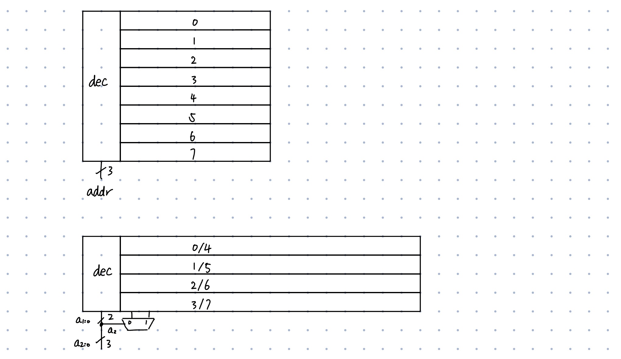
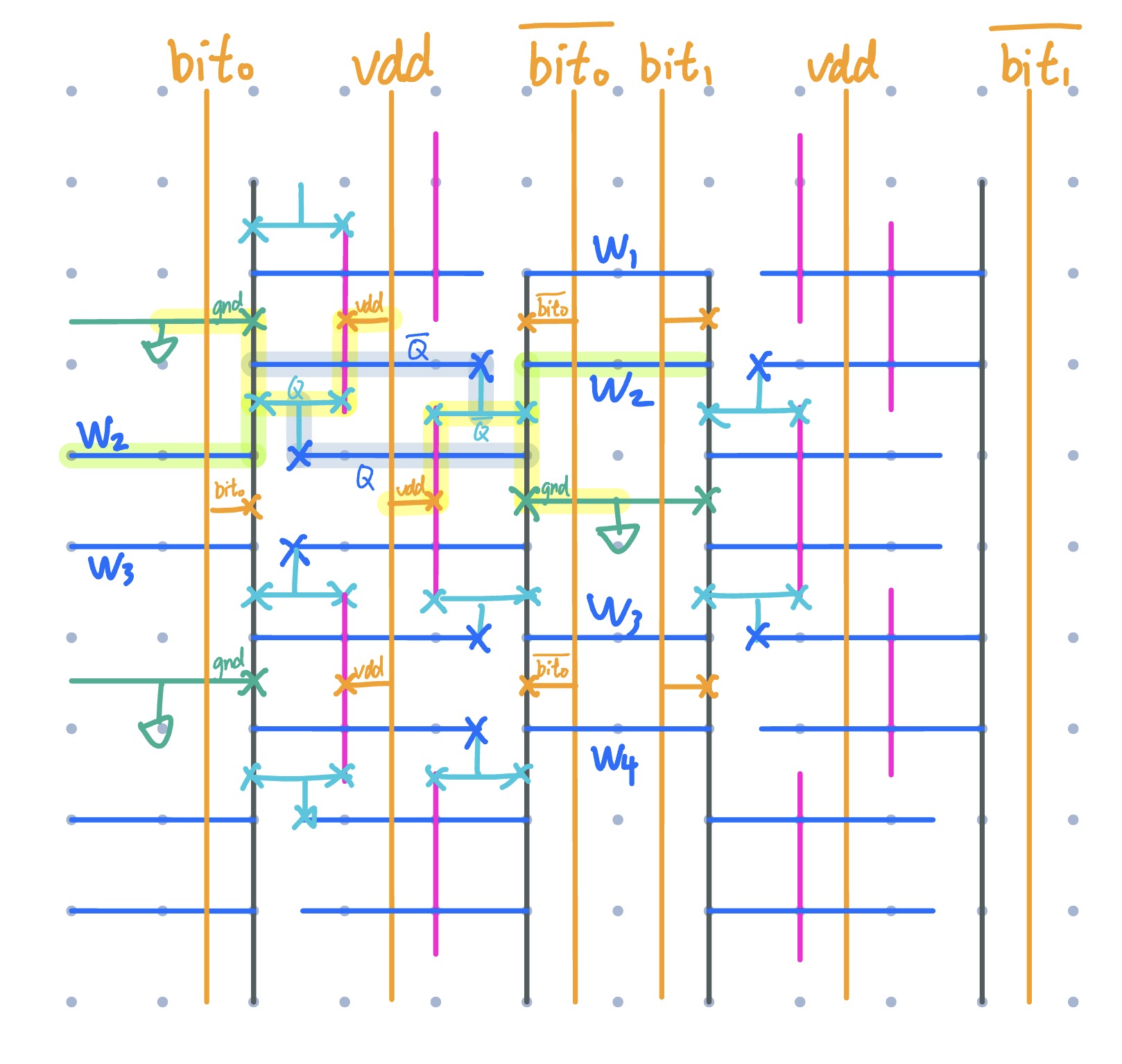
Because the SRAM cell is extremely dense, we use column multiplexing, sharing one set of R/W circuitry for each two adjacent columns
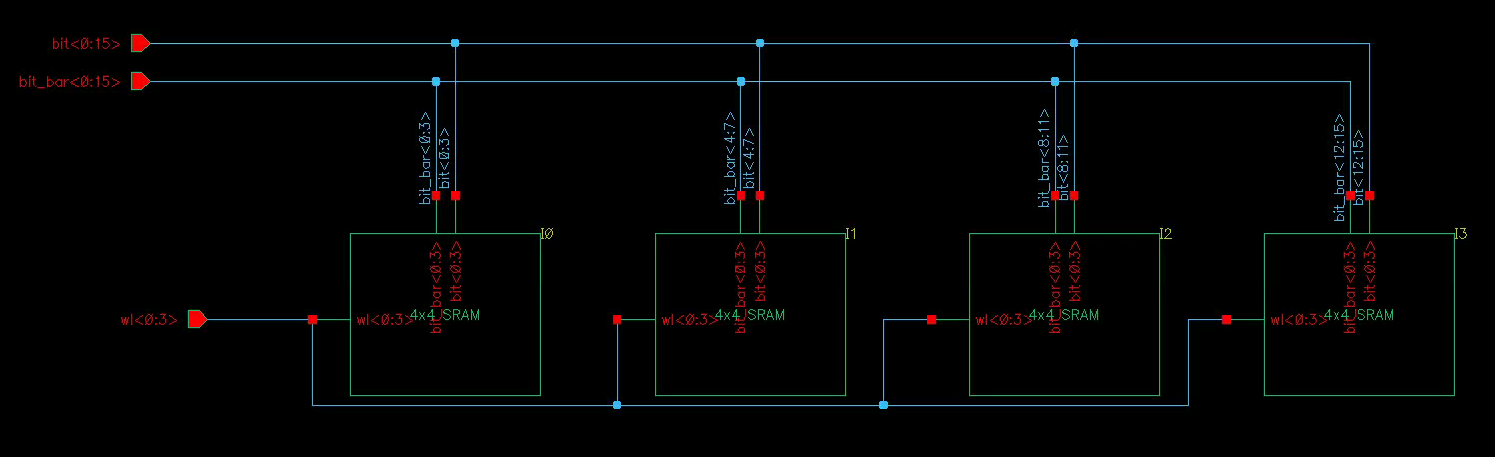
- Logically, the array is 8x8. (8 wordlines, 3-bit addresses; 8 bits for
iobus) - Physically, we lay it out as 4x16 (16 bitline pairs), where each pair of the adjacent physical column map to one logical column
- Essentially, we shift a dimension from rows into columns to the column: one wordline address bit becomes the column MUX select.
SRAM Array
8x8 Layout
The following demo array was given in Fall 2025. Take a moment to appreciate this fabulous SRAM.
Press Ctrl-F to view the blocks: 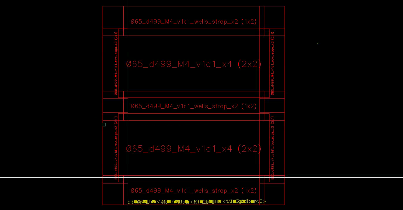
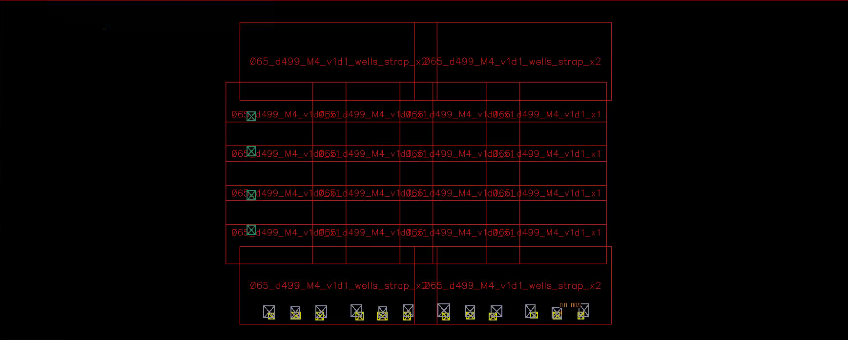
Above is a piece of v1d1_demo_array_4x4 (8x4), which contains the following: - v1d1_x1
v1d1_wells_strap_x2 (1x2)(1x4)v1d1_wells_strap_x1(power strap)
v1d1_row_edge_x2 (2x1)(4x1) (I think they are decap)v1d1_row_edge_x1(x4)
v1d1_corner_edge_x1- M2 and M4 pins
- (Fall 2025) There is an extra M3 layer at the left that will cause DRC errors. Delete it.
A level down the hierarchy: 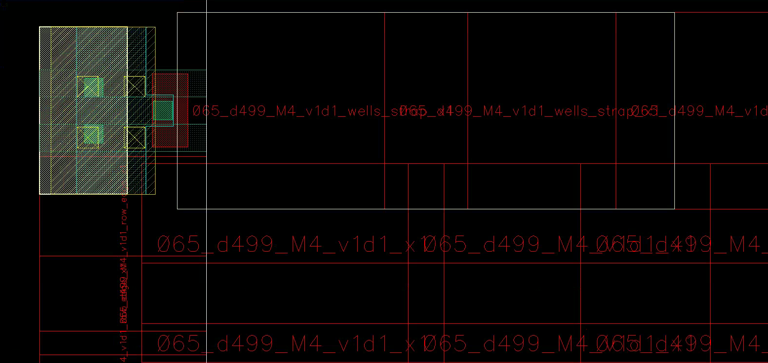
Inner Cells
Now Shift-F to show the layers. Try to hide NW and M4, analyze layer by layer, and appreciate such a fantastic design.
I annotated the cell at wordline<2>, bit<0>, clearly showing the coupled inverters and access transistors.
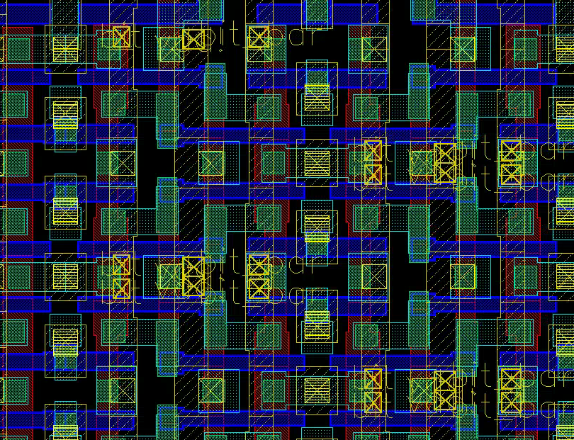
Try to make your own layout just as cute!
Don’t forget to check DRC and LVS of the SRAM cell. If there are nontrivial errors, tell Shepard to fix immediately!
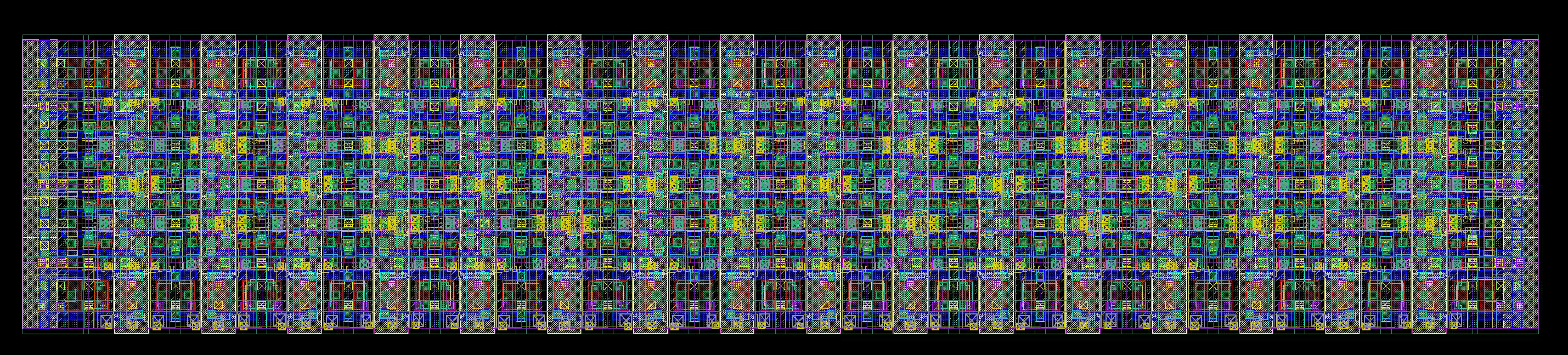
4x16 Layout
Enough appreciation—it’s time to build.
The provided 8×4 array is constructed from 4×4 blocks. Your task is to reorganize this into 4×16. As long as you understand what’s happening, this is very manageable.
You can assemble a 4x4 cell with 1x1 cells, and then piece 4 of them for 4x16.
- Make a 4x4 schematic and symbol with four
v1d1_x1symbols- 4 wordlines, bitline
<3:0>
- 4 wordlines, bitline
- Generate a 4x4 layout.
- Move entire rows/columns to save effort
- Make sure they are perfectly aligned. I’d like to look at the vias, as their sizes are fixed
- Sanity check: Does your 4x4 dimension match with the sample 4x4 layout?
- Add instances of the top and bottom
wells_strap_x2to the layout. They are not active components, so they are not part of the schematic.
- Create a 4x16 schematic and symbol with four of your 4x4
- Generate a 4x16 layout
- Add
row_edgeandcorner_edgeinstances to the layout - Again, make sure everything’s perfectly aligned
- Add
- Check DRC and LVS
- Add the pins.
- The width of the M2 wires vary, but there is a pretty clear “center line”
- Measure the distance between the center lines of
bit<0>andbit<2>. You should get 2.1 um. This is the bit pitch I’ve been talking about - Measure the M2 wires to the left of
bit<0>and to the right ofbit_bar<15>(GND). You should get 16.8 um. If not, something is misaligned. - Add M2 pins for power and bitlines. They don’t have to be perfectly square.
- Add M3 pins for wordlines and power
- Add M4 pins for power
- You don’t have to be perfect for now. We will refine later
Decoder
Shepard has probably showed off multiple decoder designs in lecture and practice exams. However, for this project, most people end up converting to a static CMOS decoder.
- With column MUXing, only two rows need decoding.
- Wordlines must be qualified with
phi_1.- Address change happens when
phi_2is high - Evaluation happens when
phi_1is high. - Multiple (even transiently) active wordlines will short the cells, leading to catastrophic data corruption.
- Address change happens when
We chose a 4-in-1 NAND-NOT layout that fits neatly within four SRAM rows and scales naturally with predecoding.
The drawback? Kind of huge in width. It will be better for this project if we can put them to a more squared shape.
The idea is simple:
- Spam M3 horizontal wires for all signals and power (Yes they fit)
- Use M2 to fetch the signals vertically from M3
- Use our M2-VIA2-M1-CO-PO stack to control the gates
- Route the outputs with M1-VIA1-M2-VIA2-M3
Implementing it is tricky, but once you have one block, the rest is simple.
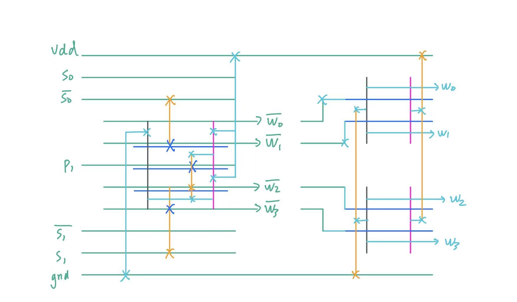
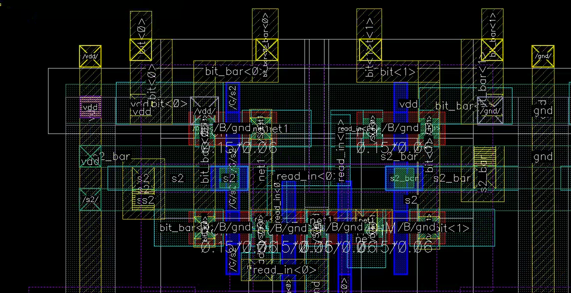
Read Write
Below is the 2-bit (4 bitline pairs) R/W schematic, closely following lecture
- Column MUX selects between adjacent columns.
- Write Select pulls down the bitliens.
- We merged the
writeanddataNMOSes to save a stack height
- We merged the
- Read Driver taps from
bit_bar, amplifies with a skewed inverter and a bus driver
Testing
Make sure the pre-extraction simulation works consistently before starting layout, so you can isolate errors as early as possible.
At the schematic level, I’ve summarized a few common failure modes based on my own experience and that of my classmates.
- Forgot to power
vdd!/VDD!/VDD.- If node voltages hover near 0V, or 0.5V, it’s very likely a power issue
- The SRAM cell implicitly uses
vdd!. After extraction, it may appear asVDD!. - At schematic level, there is a simple way to power all:
- Use 1V
vdcto drivevdd!relative tognd!. - Use 1V
vdcto tie all other powers andgnd! - Use 0V
vdcto tie all other grounds andgnd!
- Use 1V
- Wordline glitch
- Addresses much change only when
phi_2is high. - Probe all wordlines to ensure they are one-hot.
- Addresses much change only when
- Off-by-one inversion
- The lecture circuit is inverted
- Simple test: invert your input vector
- Clock phase overlap
- The circuit should work fine if
phi_1andphi_2are both 50% duty cycle. - If problems appear, try:
- Slow down the clock period
- Reduce the duty cycle
- The circuit should work fine if
- Readability and writability
- These are mostly handled in the SRAM cell.
- Make sure the transistors on the bitline add minimal parasitics.
- Close-to-minimum sizings are fine.
- Probe
bitandbit_barto see if it’s a skew issue
- Tristate issues
- Only one driver should be connected to
iobus - When writing,
iobusis driven by testbench sources. The read drivers are set tristate. - When reading,
iobusis driven by the read driver. Use transmission gates in the testbench to disconnect the testbench voltage sources!
- Only one driver should be connected to
Stick Diagram
This is legacy layout. Horizontal gates may save a lot more space
We used a vertical Poly layout for this part. You will see the pros and cons in a moment. We laid out two units at a time.
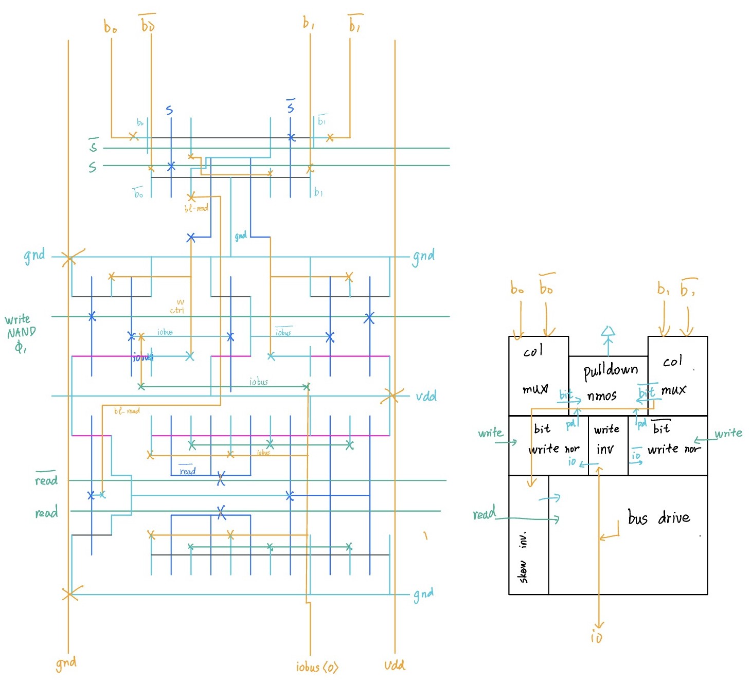
Column MUX
Four NMOS devices steer either column into the R/W circuitry.
We initially attempted a single-row diffusion-shared layout and missed by a fraction of um :( The final solution uses gate sharing instead.
A lot of wires, but also a lot of space
The pulldown path is short. Good for delay.
Write Pulldown
Now to the interesting (and hard) part. In lecture, we know that we can control the write pulldown NMOS of bit by write AND iobus (iobus_bar for bit_bar). For stability, we also want to qualify this with phi_1. The logic is:
write AND iobus<i> AND phi_1
(write AND phi_1) is the same for all bits. We can factor out the shared term and supply it from outside, drastically reducing the complexity for each cell!
And bubble push:
(write NAND phi_1) NOR iobus<i>
Omg this is too beautiful
We need iobus_bar<i> for bit_bar<i>. Fortunately, there’s ample space to squeeze in an inverter
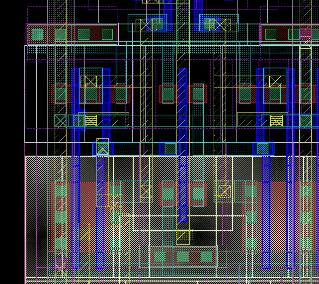
Vertical Poly allows aggressive diffusion sharing if S/D Contact and Metal is aligned directly under the M2 bit grid. Otherwise, you may waste a lot of space
Read Driver
The read driver’s pretty straightforward.
- A skewed inverter to handle bitlines
- A large tristate driver for
iobus
We chose a 4:1 width ratio. You should test it to make sure it works at schematic level.
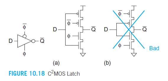
We then used a (600/300)x3 C²MOS tristate bus driver. Note that it has a stack height of 2. It is discussed in textbook pp 393
Do not add inverters after a tristate driver. That defeats the point.
With careful tuning and diffusion sharing, you can make everything perfectly fit
What if things don’t fit?
Cry, but don’t overcry. You still have to face it
- Check the basics. Start with diffusion sharing, efficient routing/viaing, avoid oversizing, etc.
- Resize device. People constantly miss that. Ask yourself: Is the device on the critical path? How slow would it be if I size it smaller? Can I finger it differently? Can I orient it differently?
- Use straight lines. Bent routes increase contention not only itself, but its neighbors as well! Try to make routes as straight as possible, or shift them away from tight regions.
- Detour. If you’ve really tried, take a detour. Find gaps on each layer, and consider moving your routing to these gaps.
- (Temporarily) move to a higher Metal layer. This is detour on another dimension. Only do this for short, local routing, as it may horribly interfere with your global routing plans. Vias are also not cheap.
- Accept tradeoffs. If there are truly no ways, you have to increase your spacing. Note that this is not an excuse to sloppy layouts.
A slightly area-inefficient design is not a failure — It’s a deliberate tradeoff. In fact, you can often reclaim the space by fitting in power straps, inverters, or decaps.
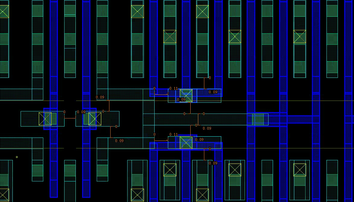 An example of diffusion sharing and detour (M1)
CONGRATS ON FINISHING HALF THE DESIGN PROJECT!!!
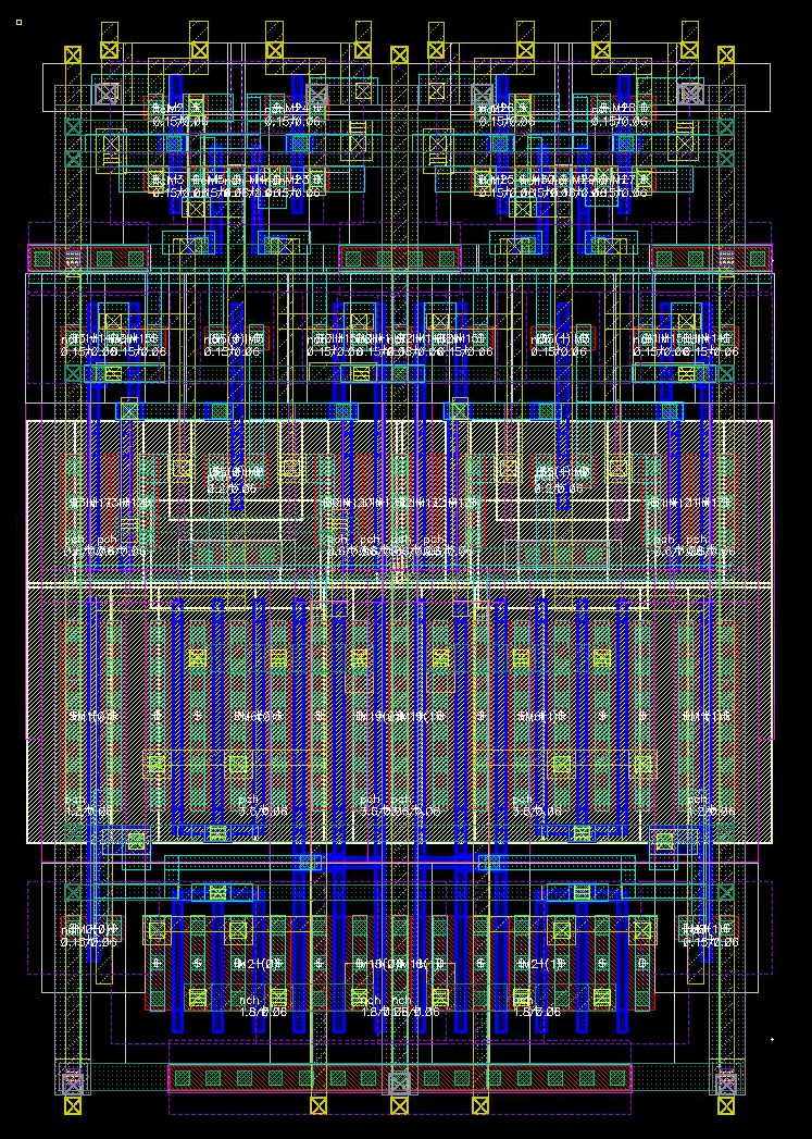
Peripheral-Peripheral
The rest of the circuit is what I call the “peripheral” of peripheral circuits, which includes:
- PMOS for cell precharge
- Logic for
(write NAND phi_1) - A couple of inverted control signals
- Power grids and pins
This is where overall layout organization starts to hurt. The main challenges are:
- Decide transistor size to drive the shared control signals
- Calculate the total fanout
- I typically make it under FO4, which is fine in practice
- I chose area over delay, not accurately optimizing large-fanout drivers.
- Find a place to place such transistors
- Find a place to prettily place such transistors
- Floorplan the grids. Integrate well with the rest of the design
Here’s how I did it:
- Draw the core transistors within the grid. Pass DRC. (proof of concept)
- Roughly connect the remaining structures (even if not DRC clean) to pass LVS (proof of concept)
- Go back and refine the details. Resolve the remaining DRC issues.
- STOP for now. Don’t try to make it perfect, as you will probably revisit it
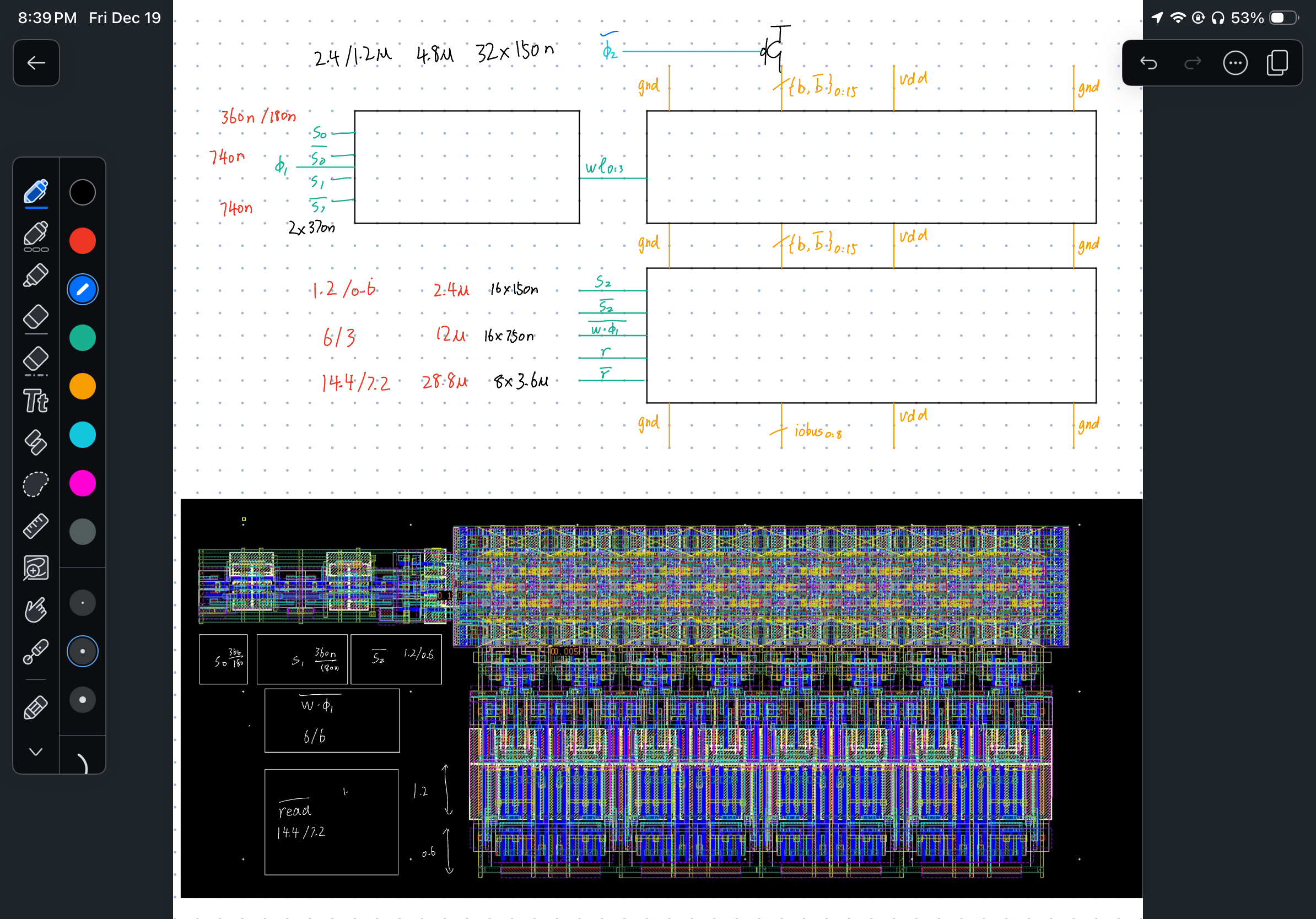
Disclaimer: these sizings are for an older version. Calculate your own!
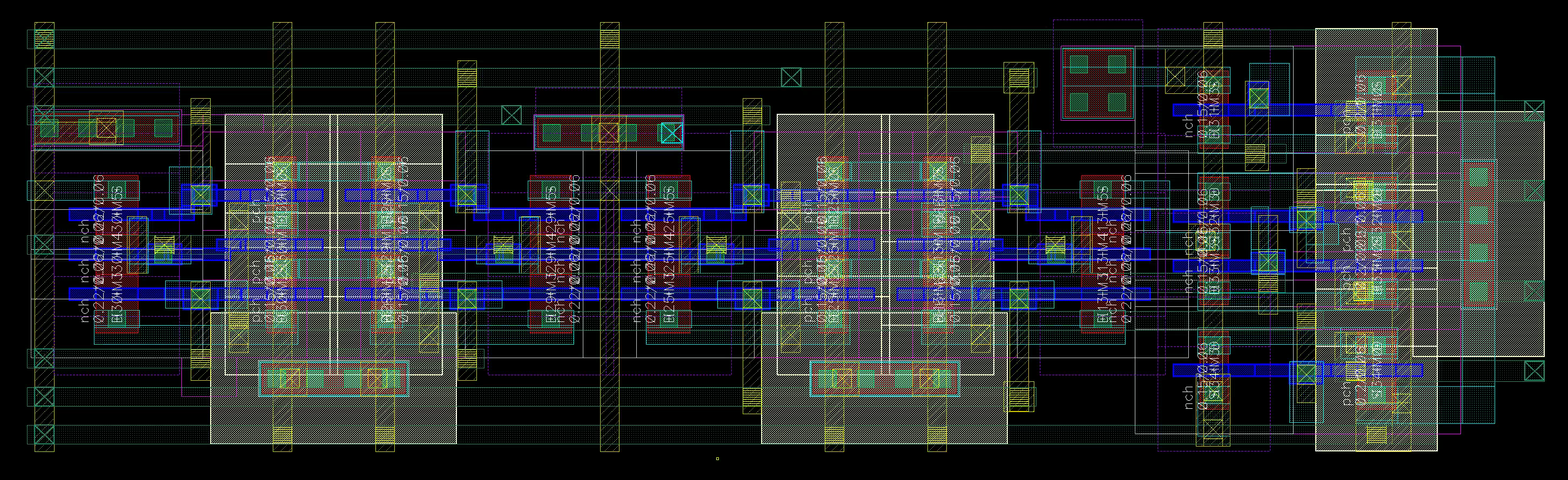
With these decisions in-place, you can lay out the whole thing: 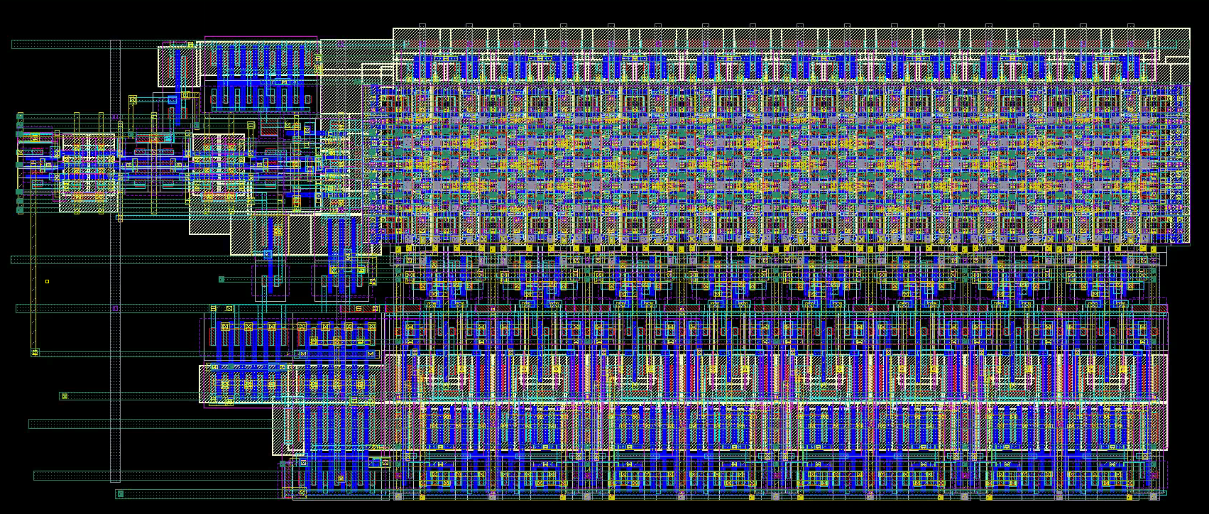
Calibre
It’s a pain dealing with third-party libraries.
LVS
You may get a few LVS warnings on M2 pin short. This is from the v1d1_x1 cells’ M2 pin label. The M4 pins are fine.
- We externally connected power through M4 and M2 at the boundary
- As long as you leave the “shorted” pins in the center untouched, it should work fine
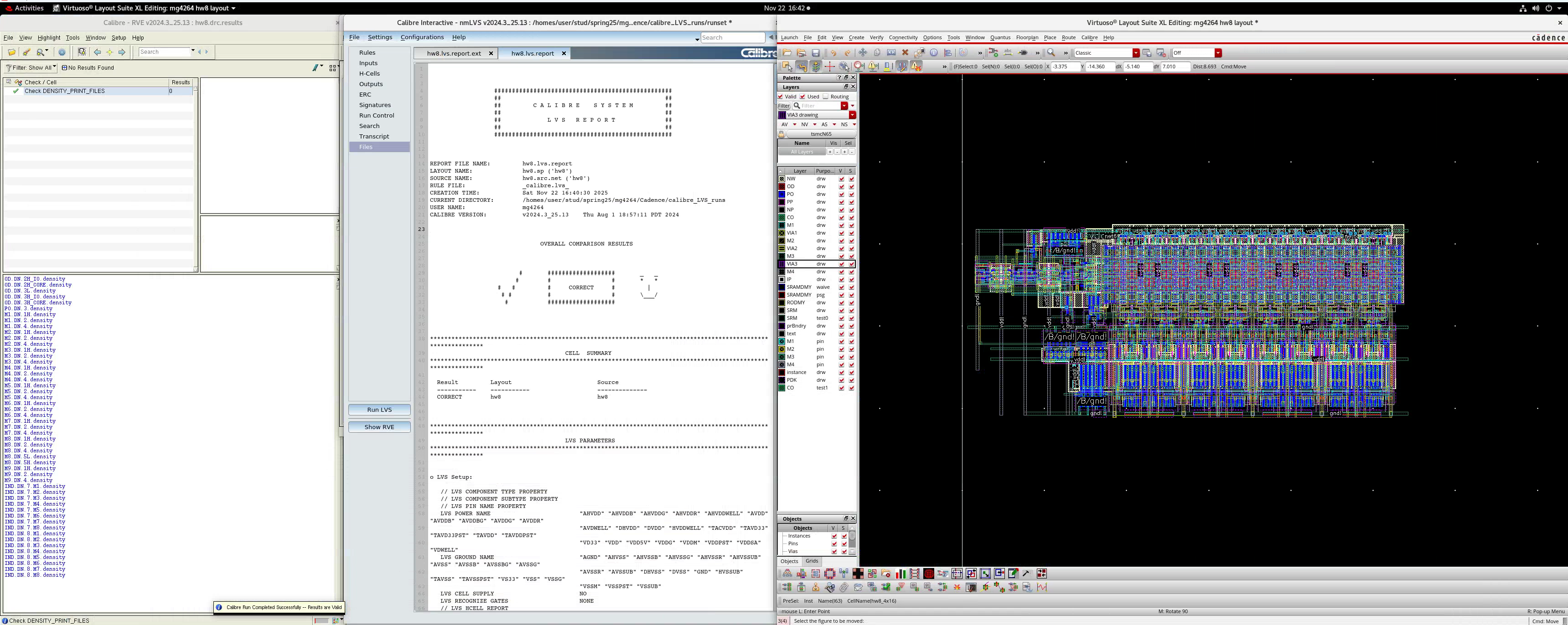
PEX
You might get the following warnings from extraction:
WARNING: [FDI3034] Schematic instance XI24/XI63/XI3/XI0<0>/M0 not found, use found instance XI24/XI63/XI3/XI0<0> instead.
WARNING: [FDI3046] Failed to create mapping for device "nchpg_sr". Netlist for "XI24/XI63/XI3/XI0<0>/M0" instance has more pins than schematic view.
WARNING: [FDI3014] Could not find cell mapping for device nchpg_sr. Ignoring instance XI24/XI63/XI3/XI0<0>/M0.
Those are fine, since the internal schematic for the 6T SRAM cell is not given. The entire instance will be used for the extraction.
- If post-extraction simulation doesn’t work, try a more tolerant testbench timing here
They post-extraction delays are around 50 ns.