
Design Project Planning
Published:
Architecture
Before even starting the project, read through the requirements so you know what you should be doing.
Our microprocessor consists of:
- Internal Bus: single writer, multiple readers
- Accumulator (Acc): A flip-flop holding temporary values
- Arithmetic: adder, shifter
- SRAM
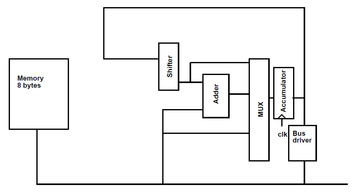
Bus
The block diagram above has two critical nets: the internal bus, and the accumulator.
- The accumulator (top net) is a flip-flop holding temporary values from the adder and shifter. Think of it as a register
- The internal bus (bottom net) routes the values to the components.
- Only one source below can drive the internal bus:
- Accumulator
- SRAM
- External bus (not shown, for testing)
- All components below may read from the internal bus simultaneously:
- Adder
- Accumulator (via MUX)
- SRAM
- External bus
- Only one source below can drive the internal bus:
Tristate buffers control data routing between SRAM/internal/external bus, preventing contention.
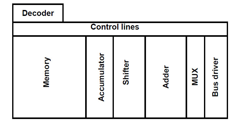
ISA
Try to derive what to do, combining with the data path above:
When holding, the value in Acc must not change. The MUX should select the shifter path, but bypass it, effectively feeding Acc back to itself
| Opcode | Assembly | Description | Internal bus driven by | MUX | Other Actions |
|---|---|---|---|---|---|
| 000 | NOP | Hold Acc | – | Hold | No change |
| 001 | LOAD | Mem[i] ← External bus | external bus | Hold | Memory write |
| 010 | STORE | External bus ← Mem[i] | SRAM | Hold | Memory read; Drive external bus |
| 011 | GET | Acc ← Mem[i] | SRAM | Memory | Memory read |
| 100 | PUT | Mem[i] ← Acc | Acc | Hold | Memory write |
| 101 | ADD | Acc ← Acc + Mem[i] | SRAM | Adder | Memory read; Bypass shifter |
| 110 | SUB | Acc ← Acc - Mem[i] | SRAM | Adder | Memory read; Bypass shifter |
| 111 | SHIFT | Acc ← Acc « shamt | – | Shifter | Don’t bypass |
Yes, this ISA is terrible for logic simplification.
And yes, there are obvious optimizations.
Floorplan
Floorplan! Floorplan! Floorplan! Many layouts don’t suck at the end, they suck at the beginning! A bad initial decision will make you either REDO from scratch, or make WORSE and WORSE compromises to accommodate that
Here is the suggested floorplan from PS9
We have laid out an inverter already. The processor can be seen as many inverter-like gates neatly coordinated.
These are the 3 main things to plan:
- Data
- Control
- Power
Metal Routing
This is Shepard’s suggested floorplan, rotated 90 degrees. I will stick with this orientation from now on
Adapt a consistent Metal routing rules. Let’s make
- Odd Metal layers horizontal
- Even Metal layers vertical.
- There can be local violations, especially at lower levels
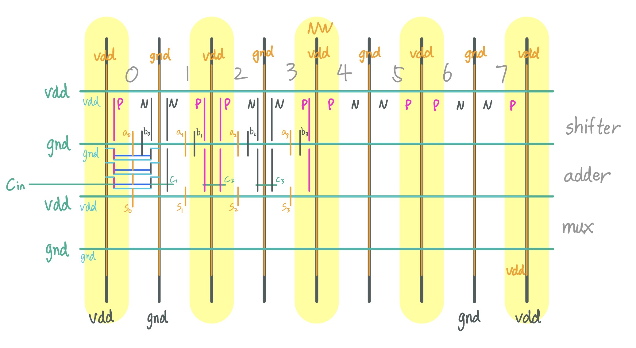
Vertical Grid
Our 8-bit processor built from isomorphic 1-bit slices placed side by side. We can create a vertical grid of M2 power rails of alternating VDD and GND
- Each cell will build VDD (PMOS N-Well) on one side, and GND (NMOS P-Well) on the other
- The power straps (body Vias) can be placed directly below the M2 rails
- All transistors will fit horizontally within each stripe. Larger transistors can be made of multiple fingers
See example in our adder
Although not done in our project, you can further design all blocks to have the same height to have an organized horizontal grid
- This leads to standard cells. You can check out some library examples!