
Columbia 4321 VLSI Project: Mini Processor
Published:
In this set of articles, I will walk through the essentials of the 4321 design project, so you can achieve an A tier layout even you are completely new to layout (like I was). It will be a huge learning curve, and that’s exactly the point.
Think of this as a process of successive approximation (Shepard’s favorite exam technique): make an initial attempt, realize how bad it is, learn something new, refine it, and repeat.
This guide is meant to help you converge faster, avoiding many of the traps and misjudgments we fell early on, and focusing on what actually matters.
Hopefully, this means less pain and suffering, but more appreciation for the real beauty of custom layout. Enjoy!
Contents
- Intro to 4321 Layout (this article)
- Inverter (PS4)
- Project Plan
- Adder and Shifter (PS6-7)
- SRAM (PS8)
- Overall (PS9)
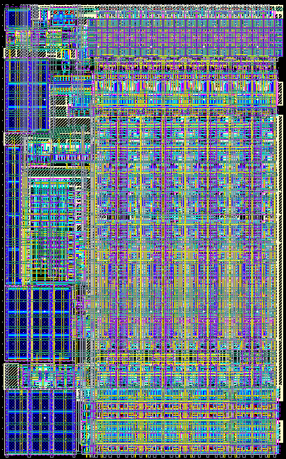
Appendix. Pictures!
Link. Offical Course Page
Link. My Class Notes
Link. Testing Tutorial by Charlotte Chen
About
Specifications:
- ~1100 µm² core area
- 4 Metal layers
- 2 GHz frequency
- 2.1 µm data path bit pitch (2 SRAM columns)
- DRC and LVS clean
Configuration:
- Static CMOS ripple-carry adder
- Transmission gate logarithmic shifter (buffered)
- 4x16 physical SRAM (static decoding, 2-column MUX)
- Pseudo-NMOS ratio PLA
- Master-slave accumulator
- C²MOS bus drivers
Disclaimer
mg-04-io is a personal blog. It is not affiliated with Columbia EE or BioEE.
This article is not an official TA guide. It’s independent from the official layout tutorials
Our project is FAR from perfect. In fact, when I was writing this, I constantly cry about how much I still don’t know about Cadence Virtuoso, and how our layout can be more efficient in this and that ways.
That’s okay.
The goal of this project is to get something done, and done well, not perfectly. This is an older technology node, intended for learning and practice, so don’t pull your hair out.
Caveats
- This guide is based on our design project. Our design evolution produces a lot of naming inconsistencies. Nevertheless, all names should make common sense and fit local context.
- Sorry for the image quality and resolution inconsistencies. Some thumbnails may not render properly. You can always open them in a new tab.
- There are suboptimal designs from the early (and late) stages of our project. I point out the obvious ones, but if you
- Spot any mistakes or inefficiencies
- Have suggestions on improving this guide
- Want to share your layout/experience
Feel free to email me at ming.g@columbia.edu. I am MORE THAN HAPPY to include it!
- These articles focus primarily on layout, but testing is equally important
- Check out the Testing Tutorial by my teammate Charlotte
- We did not explore much in Virtuoso’s design automation features. This is an area worth studying on
- This guide is never intended to help you cheat (and realistically, you can’t).
- Don’t try to reverse-engineer, as a lot of them come from our older versions
- TSMC, please don’t sue me!
General FAQ, Advice, and Folklore
This is a generic FAQ. You can find specific debugging tips in later articles
Logistics
What are the prereq?
Officially: ECircuits and Fundies
Realistically: a resilient spine, caffeine metabolism, and enough tears…
Find a good teammate.
Half of the class were having teammate issues; the other half are the teammate issues
Should I take this class for fun?
Yes, if you enjoy circuits, symmetry, compulsive optimization, or the unique pleasure of being tortured by Shepard.
Workload
Do the PSets get harder and harder?
Check out a few extremely accurate reviews from CULPA
Yes, and not linearly.
Consider PS4 the bare minimum. You will likely need a few all-nighters after that
START EARLY!!! Start them the day they are released!!!
Do they give extensions?
Not officially, but TAs are typically nice
The real question is: will an extension actually help you?
- If you are stuck on some last-minute bugs or sicknesses: absolutely
- If you are fundamentally behind: almost certainly not.
At that point, you are not buying time. You are taking out a high-interest loan… until you declare layout-rupcy
How should my partner and I coordinate?
Introducing “Out of Order Layout”:
Most of the design projects can be parallelized: design, schematic, layout, testing, and writing the report. Just make sure you can handle the “dependencies” well
Resources
Ask Prof and TAs.
Bring questions to class, to recitations, to office hours.
Ask people around you.
Your classmates know things you don’t.
They also know things you don’t know you don’t know.
Talk to them. Compare your layouts. Steal their ideas
Ask Chat.
LLMs are surprisingly helpful, especially at fetching and reading instructions and manuals. Of course, you can’t upload any TSMC NDA material to Chat to make it lay it out for you, but it is super useful at explaining concepts and interpreting errors.
What are some other resources?
There are a lot. The textbook is really good. But your brain will soon reject new PDFs.
This guide serves to distill those resources, linking the ones that I find helpful.
Design
Run DRC and LVS early and often.
Small mistakes are cheap early and extremely expensive later.
Don’t be messy.
Symmetry and consistency will save you from debugging hell. “Messy but working” layouts will stab you some point in the futures.
Don’t be perfect.
Don’t stress about getting anything perfect on the first pass. You will almost certainly revisit, modify, and sometimes completely nuke them as your design evolves. That’s part of the learning process
Don’t blindly follow Shepard.
He’s absolutely brilliant, but he’s sometimes off-by-one, whether it’s index, an inverter, or a 90-degree rotation. So make sure you understand what’s happening yourself.
What if my layout sucks?
- Before PS7: RESTART, NOW!
- After PS8: Accept your fate, BS the project, and lock in for the exams
What are some examples that suck?
- Go to StudyDocu or similar sites. Most of what’s there is hot garbage. People upload their worst work and call it “resources” :)
Go on LinkedIn, stalk some seniors and masters, check their “projects”. If they even bother putting their layout, chances are it probably sucks anyway.- I’ll also share some of our own early designs, as concrete examples of what not to do.
Grading
This class is curved, so if you are an A tier student putting in your A tier work, you should expect an A tier grade.
How will the project be graded?
Shepard will grade all projects himself, which leaves no room for BS.
This is actually a blessing compared to leaving grading to EE
TAs(more often, CAs or graders) who treat it like a paycheck task, rather than any academic responsibility.
What is the distribution?
The letter grade distribution was not published in Fall 2025, but here’s the project distribution:

It’s quite a left-heavy tail, with a similar mean to exams, but a much higher variance
- This means even though the project worths half as the Final, it has the same power to boost/bomb your final grade
How are the exams?
They are relatively easy to prepare. There are two types of exam problems:
- Freebies
These are straightforward. Some may be quite computational, but as long as you hold your ground, you’ll be fine. - Problems that “tell the boys apart from the men” (according to Shepard who’s “not trying to be sexist”)
Those are multi-part problems that require complex calculations or new concepts/equations, things that you haven’t seen. Sometimes even the TA got them wrong. Sometimes Shepard himself finds the problem unsolvable. Who knows…
Over the years, the proportion of the second type has increased, as Shepard was “running out of easy problems”
The point is: if you fail, the class fails with you. If you can’t solve the trick questions, neither can most of the class. Don’t stress too much about the exam.
I’ve thought of writing a “4321 Exam Guide,” but I don’t think obsessing over exam tricks is productive in the long run. Have a life.
- You can check out some class notes here
More to be added…
Special Thanks
Many thanks to the following for their help and guidance throughout this project:
- My teammate Charlotte Chen;
- Professor Ken Shepard;
- TAs Kaden Du, James Jagielski;
- Former students Yuxi Zhang, Yingrui Wei;
- Current students David Kim, Stephen Ogunmwonyi, Simon Mao, Nico Alarcon.
Additional thanks to William Wang on sharing his PLA layout