4321 Adder and Shifter
Published:
Now comes the first real task of 4321: adder
This is very, very important. You will learn the fundamentals of tight layout and diffusion sharing!
- Intro
- Inverter
- Project Plan
- Adder and Shifter
- SRAM
- PLA, Control, Data, Overall
Overview
- Use ripple carry
- Make a (rough) stick diagram before you start
- Fix a bit pitch of 2.1 um
- Edge DRC
- Diffusion share, and if you can’t, put as closely as DRC allows
- Do not use the default Vias
- Leave room for upper-level Metal routing
Below are some improvement areas in our implementation. Don’t copy them blindly.
Adder
- More organized M2 data grid
- Use minimum sizing on the non-critical path PFETs
- Better diffusion sharing with S/D swapping
- Using inverted
COUTto save a gate in the propagation path- MUX-based
SUBselect- Use an odd number of fingers for better diffusion sharing
- Fewer, more organized body vias
- An organized M3 and M4 power grid
Shifter
- Since we are buffering all I/O, we can do the MUX with NMOS only
- You can save some space by routing the inter-block connections on M3, instead of M1. and a lot of more…
Design
Ripple carry is simple, yet more than sufficient for this 8-bit project.
A ripple carry adder/subtracter has 3 parts:
- Subtraction inversion
- Carry generation
- Sum generation
The CMOS implementation is pretty standard, and you can find plenty of resources
Sizing
Textbook page 432 shows the standard sizing. Carry propagation is the critical path; all other paths use minimum sizing.
The suggested minimum width of is 150 nm
- Below that, the MOSFETs will turn into a dogbone shape, which actually takes more space!
We used the following sizing:
- Critical path: 300 nm * 4 / 150 nm * 4
- Non-critical path: 300 nm / 150 nm
- It’s a better idea to size the PMOS to 150 as well :( We went lazy…
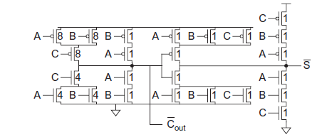
Schematic
Below is our carry schematic. If you want to use the textbook sizing, change the non-critical path NMOS sizing to 150 nm.
A few notes:
- Use multiple fingers, so every transistor has equal width
- Set up one P/NMOS with the parameters, then duplicate them over
- Connect all PMOS bodies to
VDD!, NMOS bodies toGND!. No exception - Label the nets and explicitly add the IO pins
- I recommend using capital letters for net names, and global
VDD!/GND!
I will refer to transistors by their name
Mxin the schematic above. They will differ in your schematic
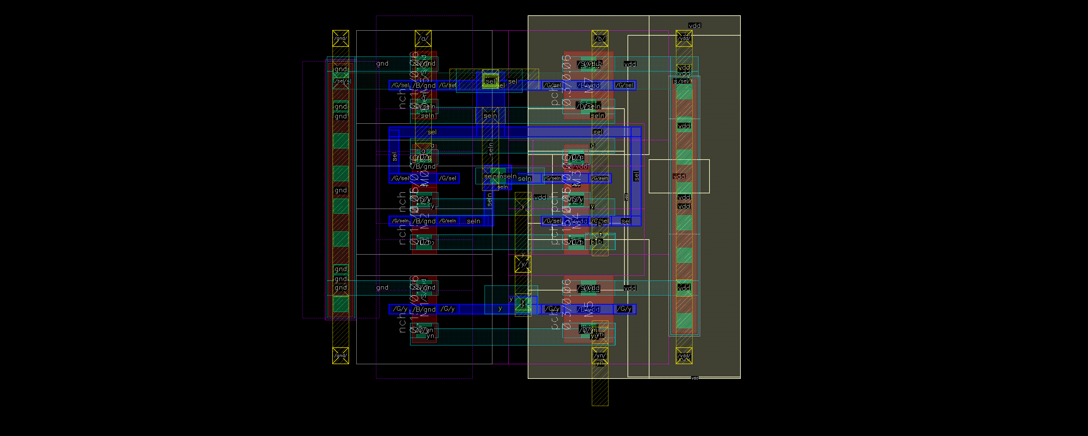
Stick Diagram
Make a stick diagram of your adder layout. This UMich lecture is pretty useful. Adapt it to your design.
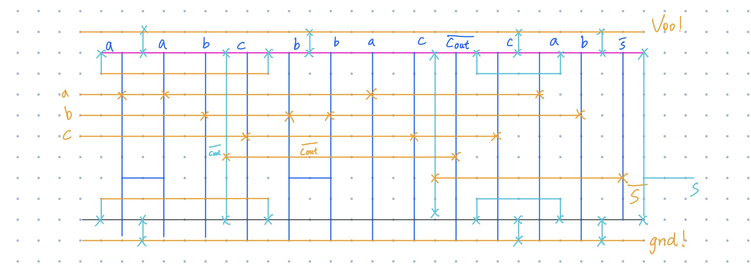
This stick diagram is rotated 90 deg. In the actual layout, M2 (orange) will be vertical. I used magenta for PMOS OD, and dark gray for NMOS OD.
For simplicity, I only show one finger. Multiple fingers will differ slightly in diffusion sharing
Alternatively, you can give up planning and “vibe layout”, sometimes not bad
Carry Circuit Walkthrough
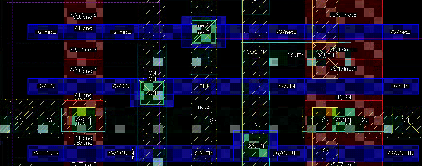
Similar to the inverter, “Generate All From Source.” You will get a sea of transistors and pins from the schematic. Our job is to move and connect them correctly.
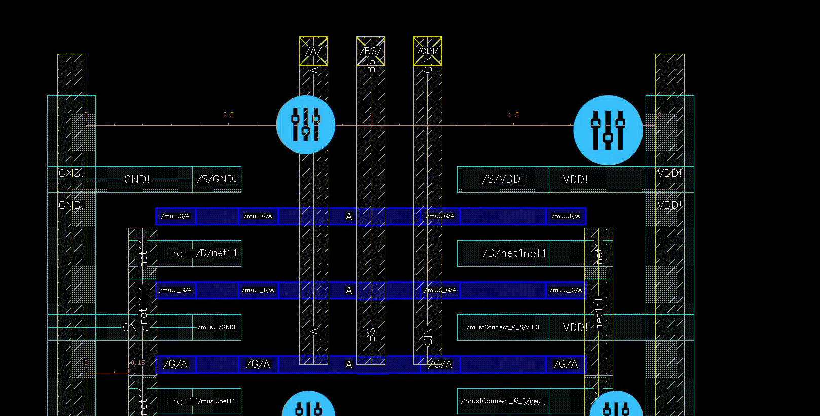
1. Bit Pitch!
Before placing anything, draw your M2 bit pitch.
- Center-to-center: 2.1 um
- Width: 0.1 um
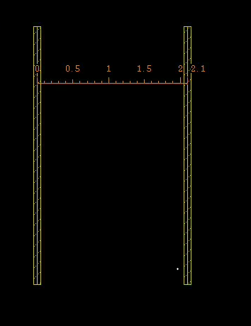
You can use the p shortcut to draw a path. It shows its DRC boundaries, too
2. First Transistor
- Find the two fat 8/4 transistors gated by
A. - Move them within the M2 grid, and rotate properly.
- Make sure PP and NP touch, but not overlap
- Add the M1-NW and M1-SUB vias.
- Align their centers with the M2 grid!
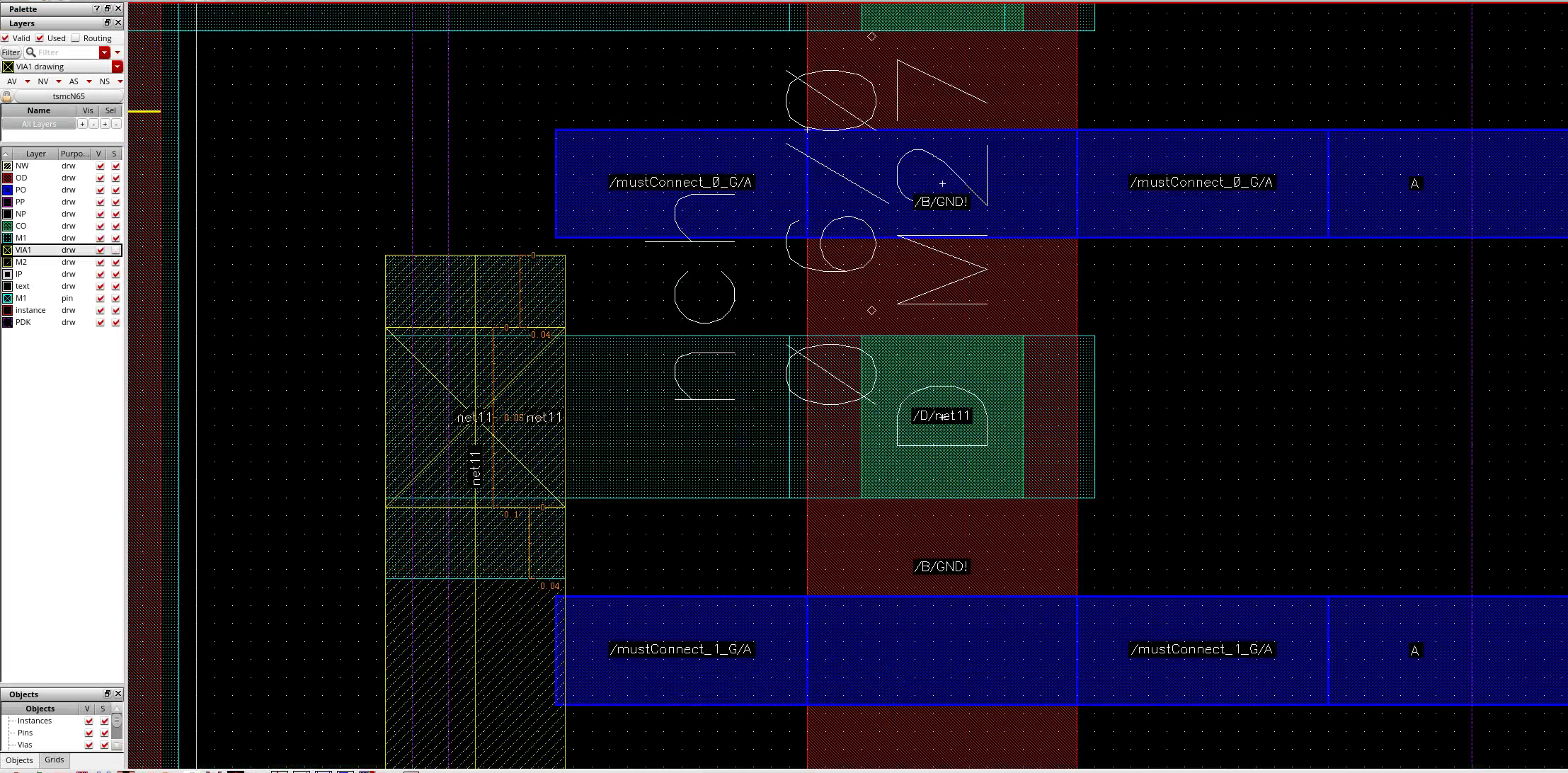
3. Diffusion Sharing
Find the single-fingered transistors gated by A.
- The top terminal (S) should be connected to
GND!, so does the bottom terminal (S) of the four-fingered device. - We can make them share the same diffusion
Move the transistors together: 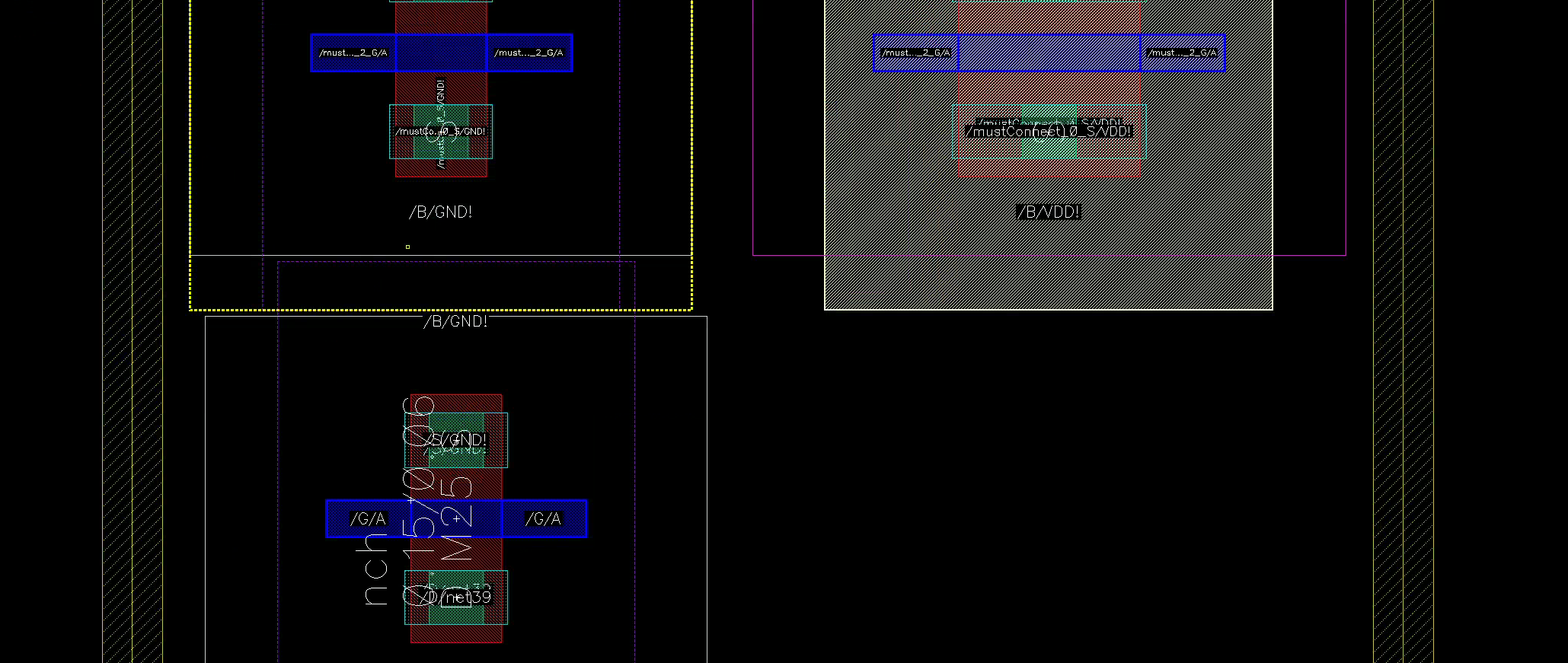
Move the bottom transistor further up, and release your mouse. Virtuoso should snap them together. 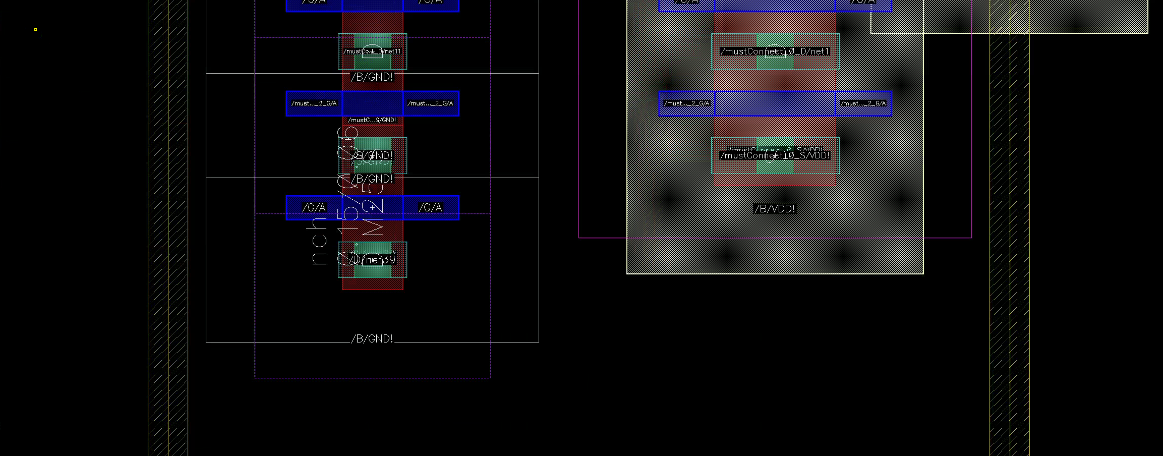
Repeat for the PMOS.
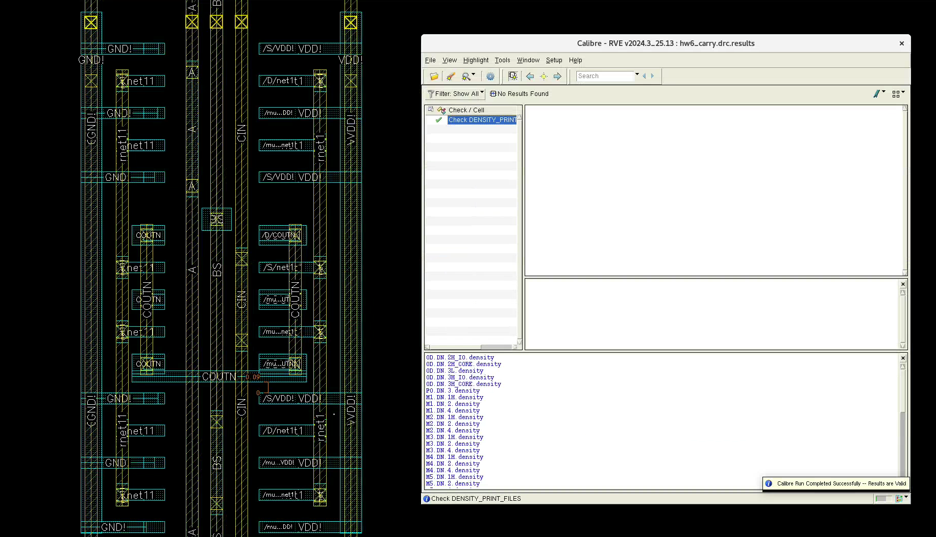
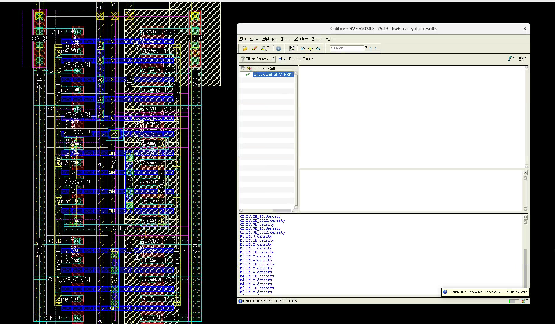
Now, check DRC. I would recommend temporarily deleting the transistors you haven’t yet placed, so their DRC disconnections doesn’t obstruct any actual errors.
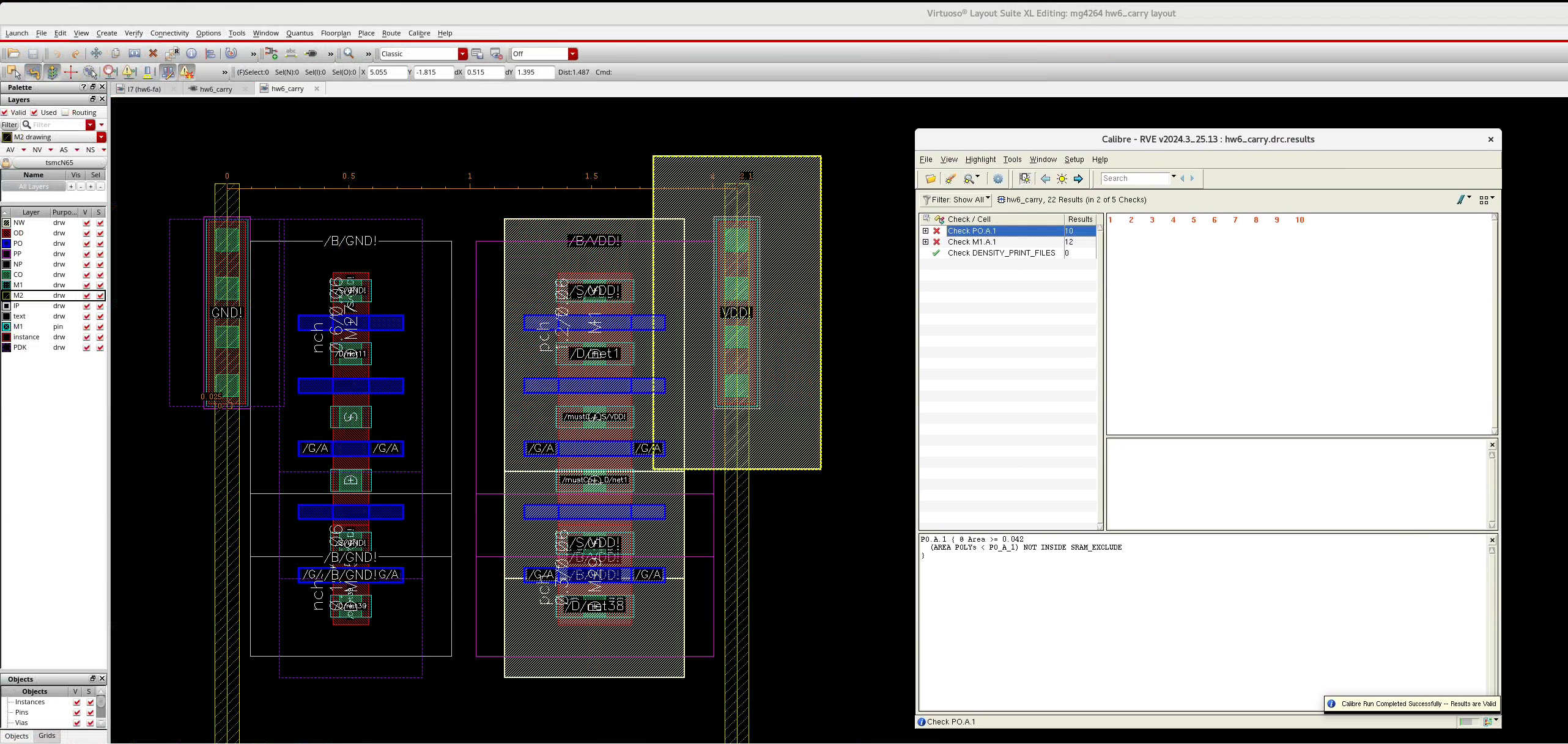
You will get quite a few errors. It’s complaining that the M1 and PO areas are too small. That’s fine, since we haven’t connected them yet
Now, restore the deleted transistors by “Connectivity/Update All From Source” (not Connectivity/Generate)
S/D Swap
For M30/M5, with its drain to COUTN. However, the generated instance has its source net1 on the outside. We need to swap the source and the drain.
- Select the FET, click
q - Go to “Parameter”, check “S D swap”
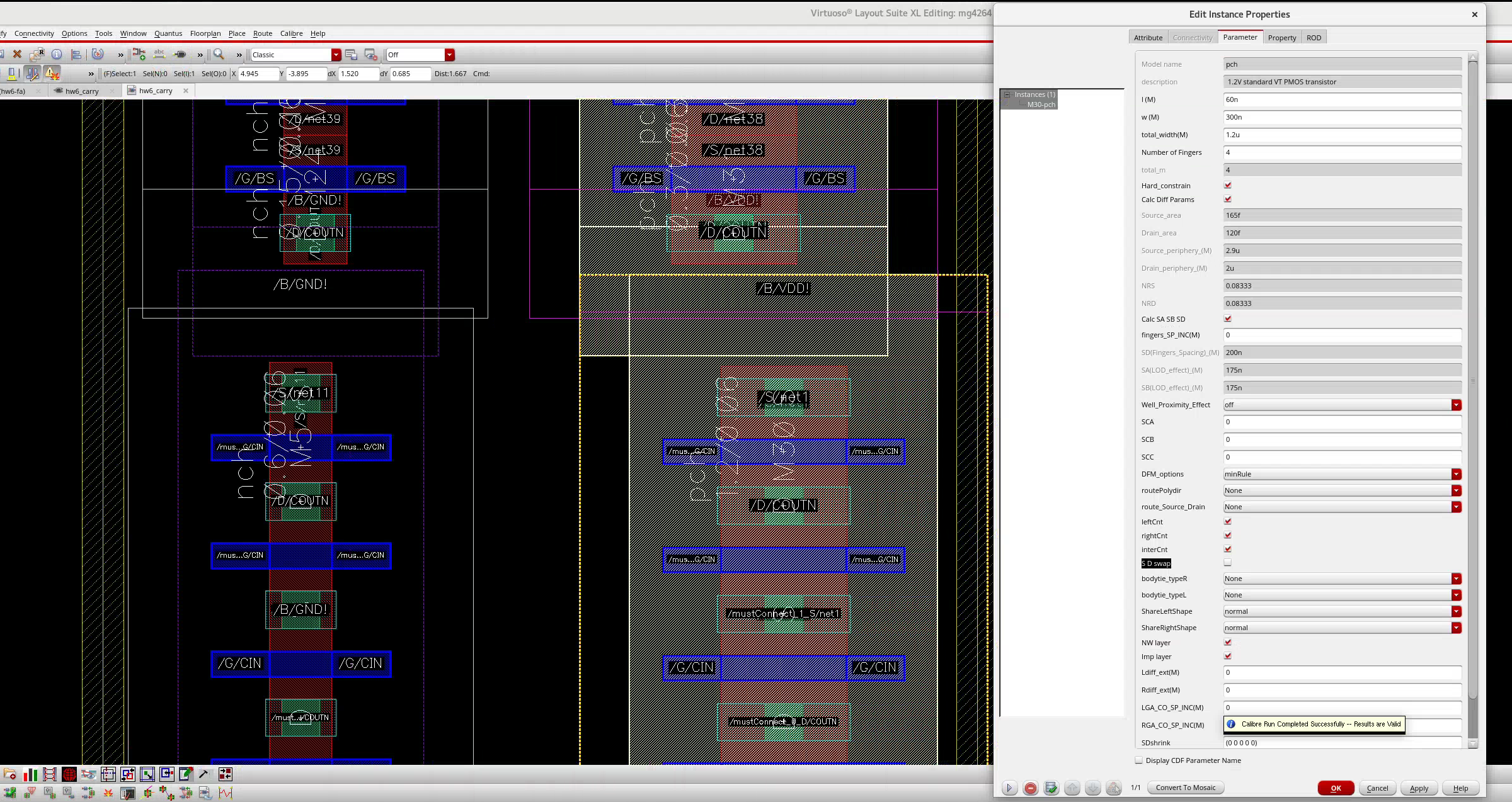
Now you can happily diffusion share!
4. Non-sharing Neighbors
Most people fuck up on this one. They start crying once they can’t diffusion share
We run out of diffusion shares for M28/M26, a suboptimal situation.
The key is to know what can still be overlapped, and what can’t.
- The bodies (NW/PP/NP) have the same potential. They can overlap.
- The active regions (PO/OD) regions are different nets. They need to be 0.13 um apart
- This happens exactly when the PP/NP boxes overlap with the neighboring OD
Check DRC again.
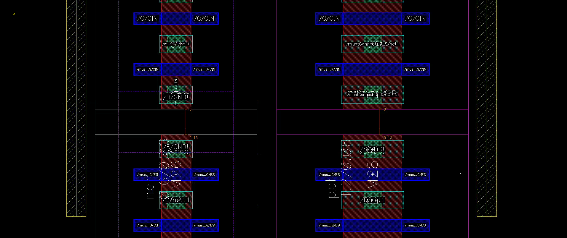
5. Simple connections
Now let’s make DRC pleased by connecting the simple poly and metal wires:
- Draw an M1 rectangular extension from the
VDD!/GND!vias- Place M1-M2 vias (make sure they are 0.1 um squares)
- Draw rectangles, or paths, to connect every S/D labeled
VDD!/GND!to the supplies - Draw poly paths to connect every poly with its neighbor
Check DRC again.
- All PO area issues should go away, as well as some M1 area issues.
- You will get a PP enclosure error. Draw a PP rectangle to perfectly cover the PP-NP gap in the center.
6. M2 Connections and Vias
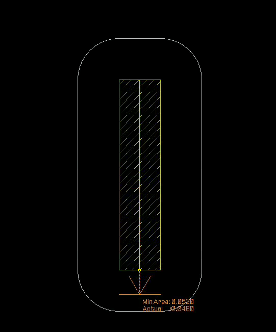
We still have a few sources and drains left. Let’s route them vertically using M2 layer. Draw a single M2 wire with minimum width (0.1 um).
I do not recommend using the vias generated with
o. They are too fat and ugly, and they are the root cause of DRC miseries if used improperly. Instead, let’s manually construct the M1-VIA1-M2 sandwich
- Select the VIA1
drwlayer. Draw a 0.1 um x 0.1 um square at the intersection - A VIA1 requires enclosure by both M1 and M2, of either:
- 0.04 um on 2 opposite edges (almost always preferred)
- 0.03 um on all 4 edges
- Use the ruler tool (
k) to measure 0.04. Usesto extend the both layers.- You may be tempted to extend M1 to the left, but that will violate the M1 spacing rules with the
GND!wire.
- You may be tempted to extend M1 to the left, but that will violate the M1 spacing rules with the
- Done! Check DRC
Do the same thing for other nets. You can also use the same technique for power and ground connections.
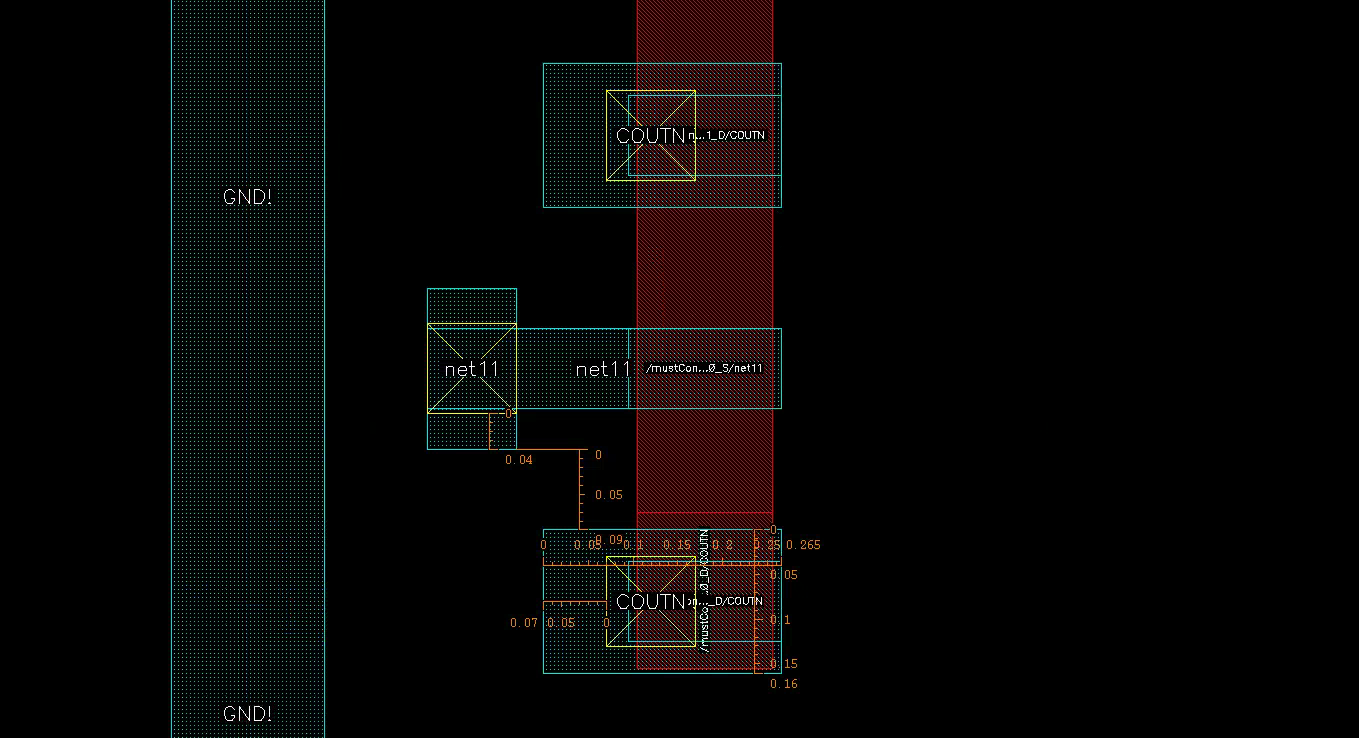
7. PO Connections and Contacts
From our floorplan, our input signals A, BS, CIN will arrive from the vertical M2 layers. We can “Update/All From Source/IO Pins” to create M2 pins and label them.
We need to via from M1 all the way to PO. There needs to be five layers: M2-VIA1-M1-CO-PO. Each must satisfy the design rules:
Be aware of the following common design rule violations (all units in powers of um)
POspacing > 0.12M1spacing > 0.09; 0.11 in cornersM2spacing > 0.10; 0.12 in cornersM1area > 0.042M2area > 0.052COside length = 0.09VIA1side length = 0.10COmust be enclosed byPOby > 0.01;COmust be enclosed byPOby > 0.04 on opposite sides; or > 0.025 on all sidesCO/VIA1must be enclosed byM1by > 0.04 on opposite sides; or > 0.03 on all sidesVIA1must be enclosed byM2by > 0.04 on opposite sides; or > 0.03 on all sides
The layout should be straightforward, although there may be a lot of trouble when working with custom Contacts and Vias.
The single BS gate in the middle is especially hard to contact:
- Any vertical PO extension 0.04 um from the CO will violate the PO spacing rules. Therefore, we extend the PO horizontally.
- The M1 island is too small. Extend it so that it covers the CO and M1 without violating spacing rules with its neighbors
Those tricks will come up repeatedly later :)
Check DRC. Below I show the PO-CO-M1 layer for more clarity: 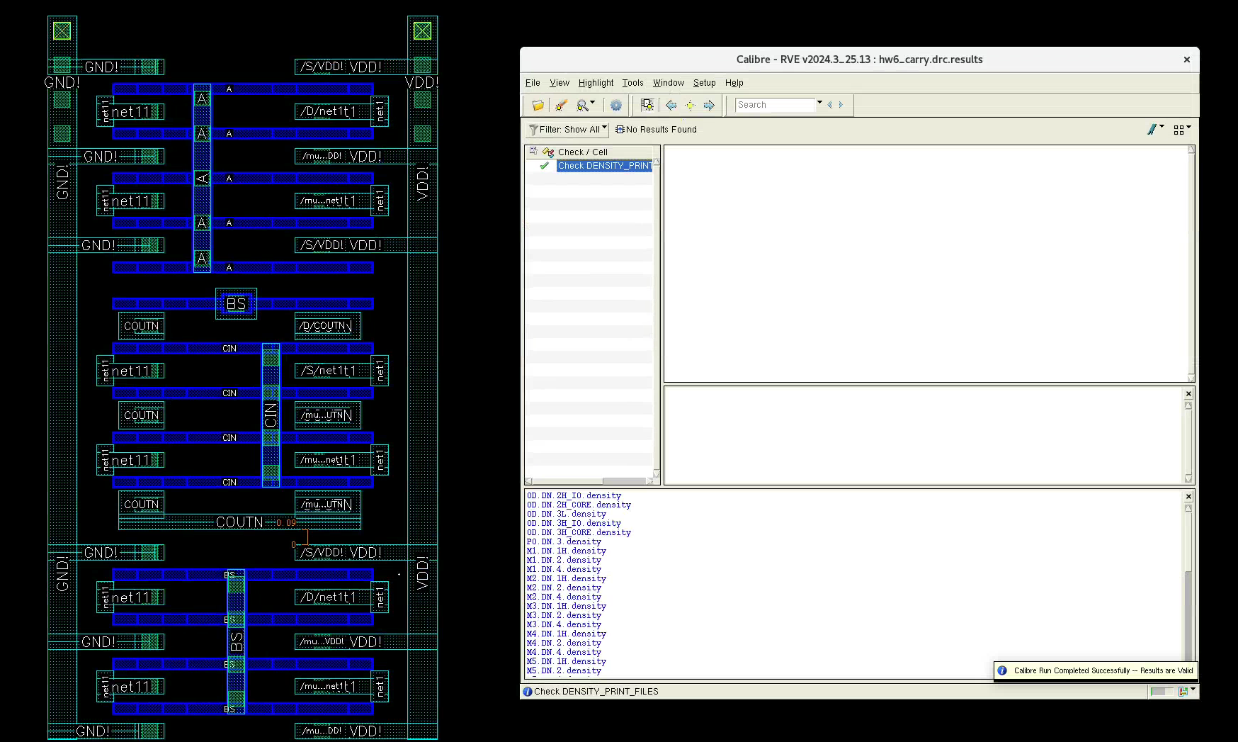
Measure the distance to its neighbor. Clean!
I also added the M2-M1 Via to connect the power.
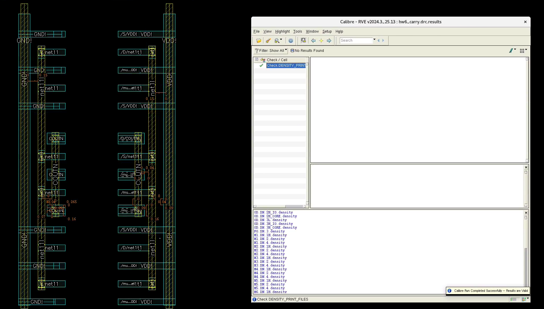
Once you add the Pins, you should pass LVS too!
CONGRATS on completing 1/3 of this assignment!
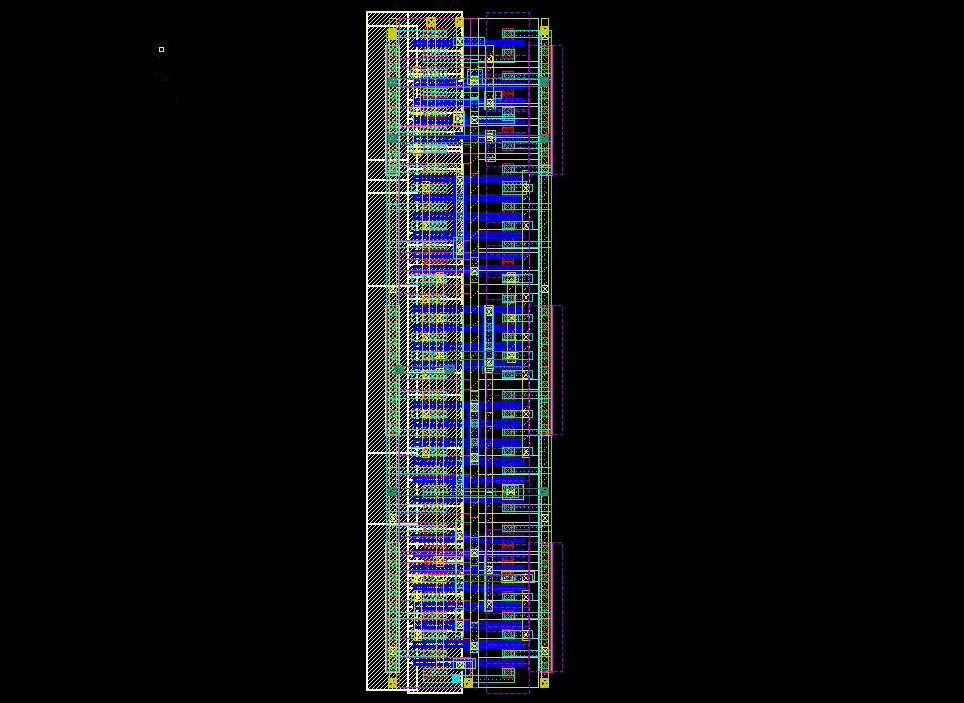
1-Bit Adder
Below is our adder from a few months ago.
Sum
The sum bits use minimum P/N sizing. They can be really well diffusion-shared!
We can closely align the PO, M1, and M2 layers
Subtraction
You can implement subtraction in two ways
- Static XOR gate
- MUX
We chose the XOR implementation.
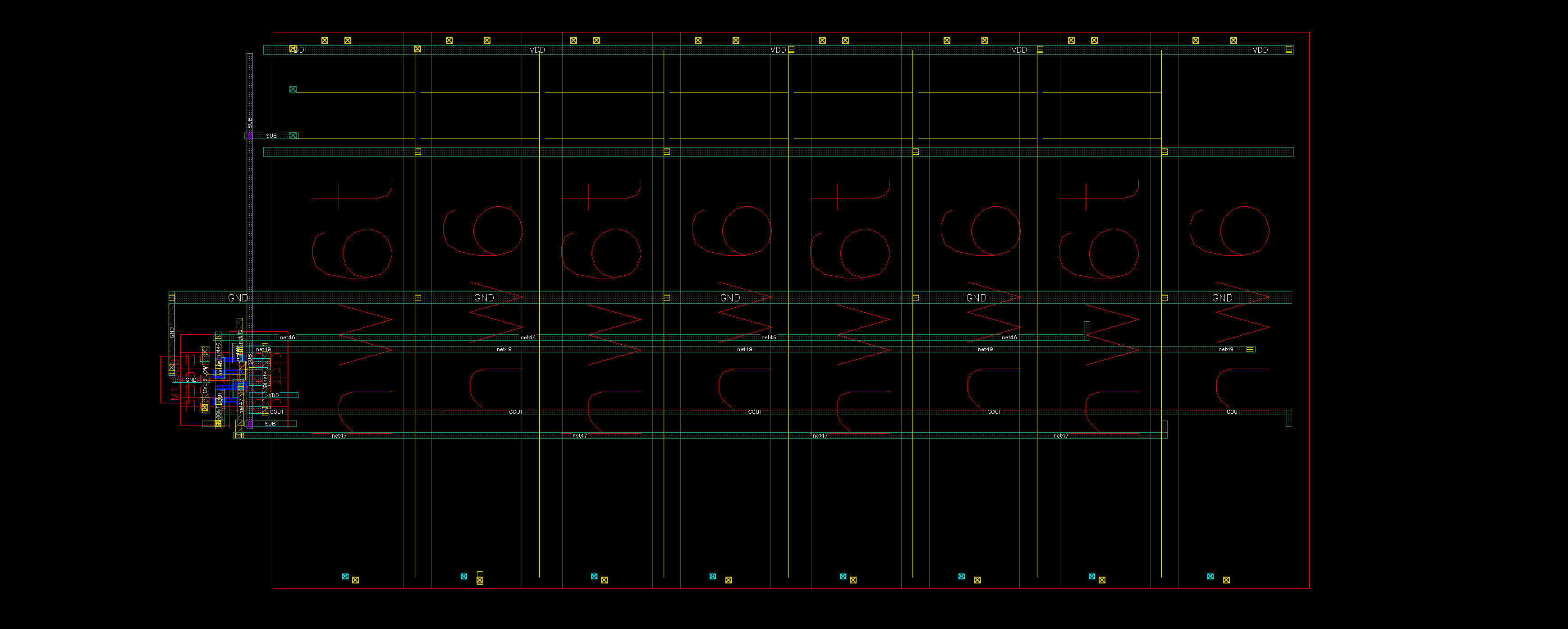
8-Bit Adder
This is very important. You do not want to draw this eight times. Fortunately, we can Instantiate (i) the single-bit layout as a symbol, just as the pch and nch symbols.
Flipped Adder
Because we use the alternating VDD-GND-VDD-GND-VDD power grid plan
- Odd bits: GND left, VDD right
- Even bits: VDD left, GND right
You can simply “Flip Vertically”. Can you?
Mostly yes, but with the caveat on pin order:
- Our current M2 pins have “ABC”, which will turn to “CBA” if flipped.
cincurrently comes from the left, andcoutfrom the right. They need to be flipped.
We created a new schematic and layout hw6t for the flipped version by copying (c) the hw6 layout, flipping it, and adjusting the pin orders appropriately.
There are definitely other ways to do this:
- Enforce symmetry for simple layouts
- Build schematic and layout for 2 bits at a time
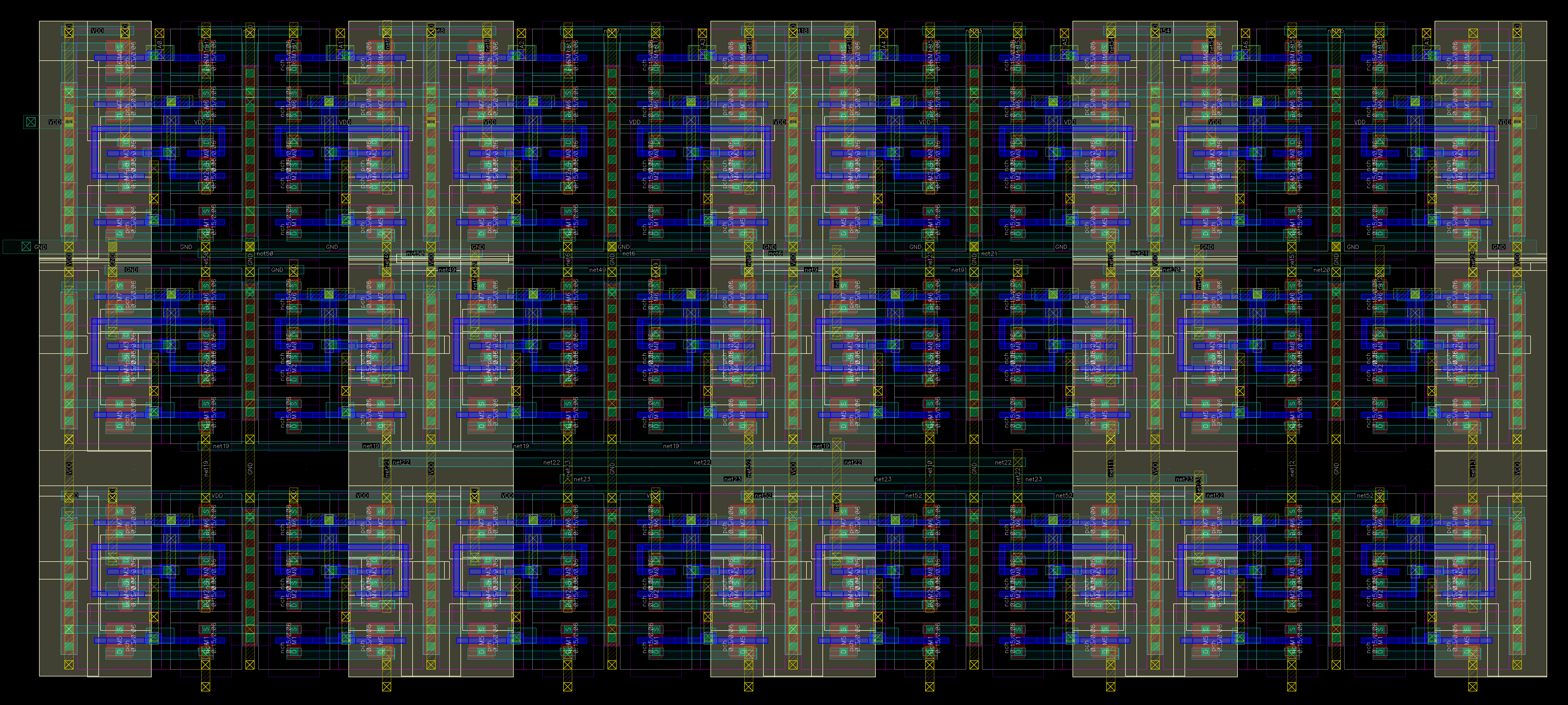
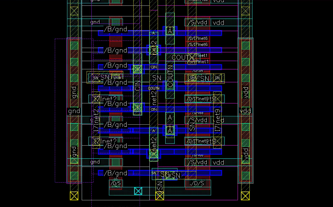
Layout Hierarchy
Now the final push! We want a coherent pattern and minimally wasted space. If you lay out your single bit like this, it’s gonna suck. You want it as tight as possible
- Make sure your single-bit layouts are DRC and LVS clean
- Create a symbol your single-bits. It doesn’t have to be fancy
- Create a new 8-bit schematic. Connect the bits with alternating
hw6tandhw6
- Check and test the 8-bit schematic on the sample inputs
- Create a new layout 8-bit, with the same name as the 8-bit schematic.
- “Generate All From Source”
Virtuoso will generate the 1-bit instances. We need to connect them.
Layouts communicate across hierarchies through Pins. If you zoom into the Pins, you will see it’s labelled. For example, “/SN/SN7”
- “/SN” is the internal net name (sum out)
- “/SN7” is the current net name (7th sum out)
- Wires connected through a pin are automatically labelled by Virtuoso.
- Wires connected, but not through a pin will still be the same net, and checked equally under DRC/LVS. Just harder to see.
In the case above, the bottom M2 VDD is connected through a pin and labelled. The top M2 is also connected, but not labelled.
- If you want the top M2 to be labelled as well (say you misaligned the pins), simply draw another M2 segnment overlapping the instance M2 from the pin (no worries, they are the same layer).
Alignment
Now the hairy part: align each bit perfectly. Fortunately, our design accommodates exactly that.
Make sure neighboring M2/M1/vias/pins overlap exactly, both vertically and horizontally.
- The M2 center points between both ends should be 2.1 x 8 = 16.8 um. If not, you’ve done something wrong.
- Your 8-bit layout will have a P-N-P-N-P-N-P-N-P structure
I went up to M3 for the carry propagation wires, but you may as well do it in M1. The M1 power/ground vertical wires do not have to be contiguous. We can via local M1 wires from the M2 power lanes.
It is good idea to use M3 for global control signals, such as SUB
Here’s how it should look like:
Overflow
Get c7 and c8 from M3. In our top-level layout, I placed the control logic near the LSB, so the overflow signal needs a long detour. It’s cleaner to place it as the MSB
Do a C+CC extraction only. RCC might crash Cadence
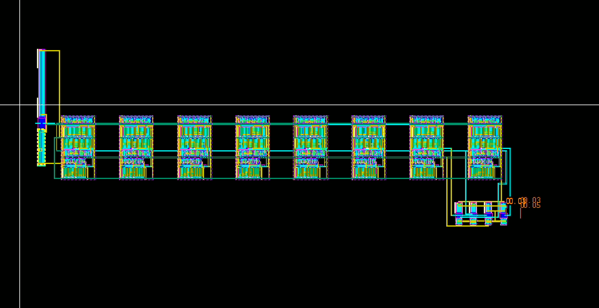
Shifter
There’s nothing too much to write about the shifter. It’s not very interesting.
We choose a complementary pass transistor MUX for our shifter. You can also choose an NMOS-only version.
Sizing
Textbook page 351-352 covers pass transistor effective resistance, sizing, and layout:
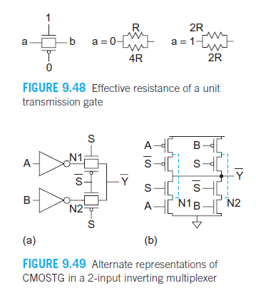
Stick Diagram
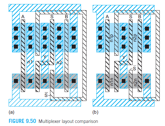
We chose to buffer at each MUX data input/output to reduce the effective stack height.
Layout
You can see the iconic “alternating gates”: