
4321 PLA, Data, Control, and Overall
Published:
Now for the final push!
Again, most of this can be done in parallel via successive approximation (aka trial-and-error) toward an optimal layout. However, plan your PLA and data path carefully before touching Virtuoso. Good planning speeds up convergence :)
- Intro
- Inverter
- Project Plan
- Adder and Shifter
- SRAM
- PLA, Control, Data, Overall
Power Grid
Make sure the entire chip have a robust and continuous power grid. Route power nets all the way to the highest Metals.
- Data path is already fairly structured. You can add a few straps if space permits. Do it last, though
- Control path: Try to maintain some regularity, but due to the lower transistor density, it doesn’t have to be as dense.
- Make sure all Vias are properly connected and not shorting out
Data Path
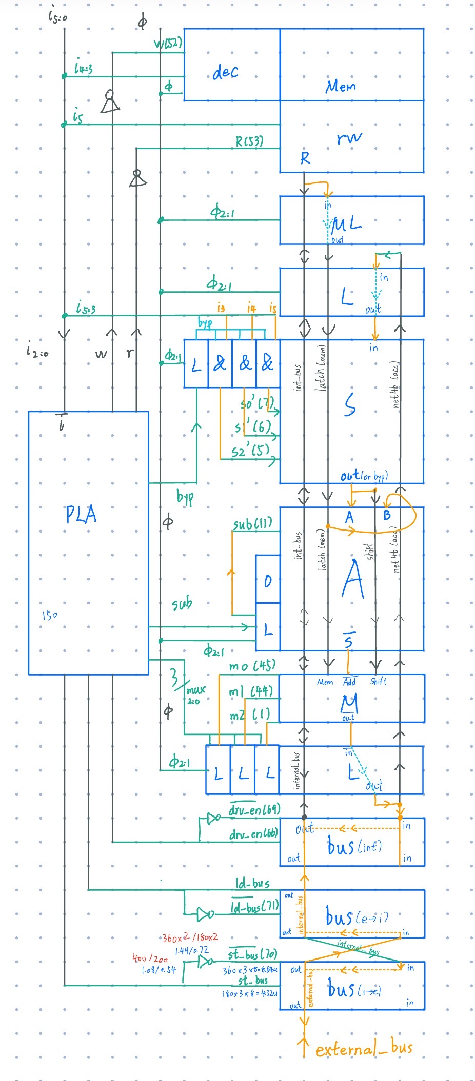
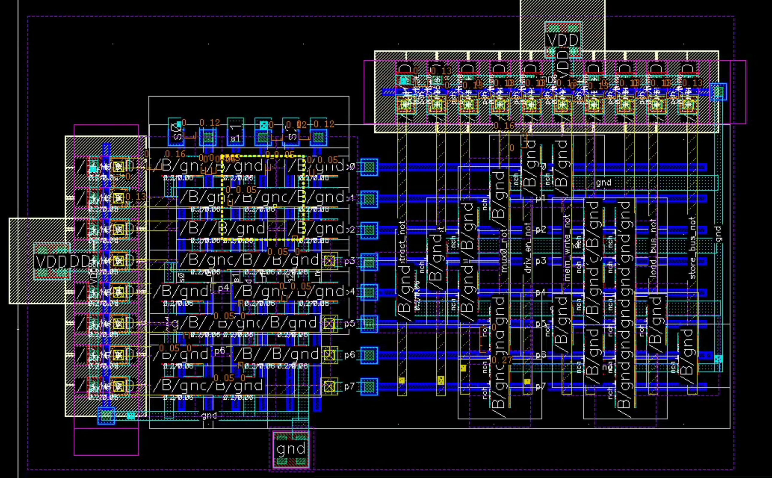
Here’s a detailed floorplan derived from Shepard’s PDF, following all his implementations
- “ML” is the
phi_1latch from the memory - “L” below it is the
phi_1latch from the bottomphi_2latch
There are three main “bus-like” nets
Acc: the state stored between thephi_2andphi_1latch, denoted as “net46 (acc)”, operated by all arithmetic unitsinternal_bus: connection between the accumulator (arithmetic), memory, and external busexternal_bus: external IO
There are a total of 4 bus drivers:
- Accumulator → Internal bus
- External bus → Internal bus
- Internal bus → External bus
- SRAM → Internal bus (done)
Possible optimization: feed the external bus directly into the MUX to reuse the Acc → Int driver
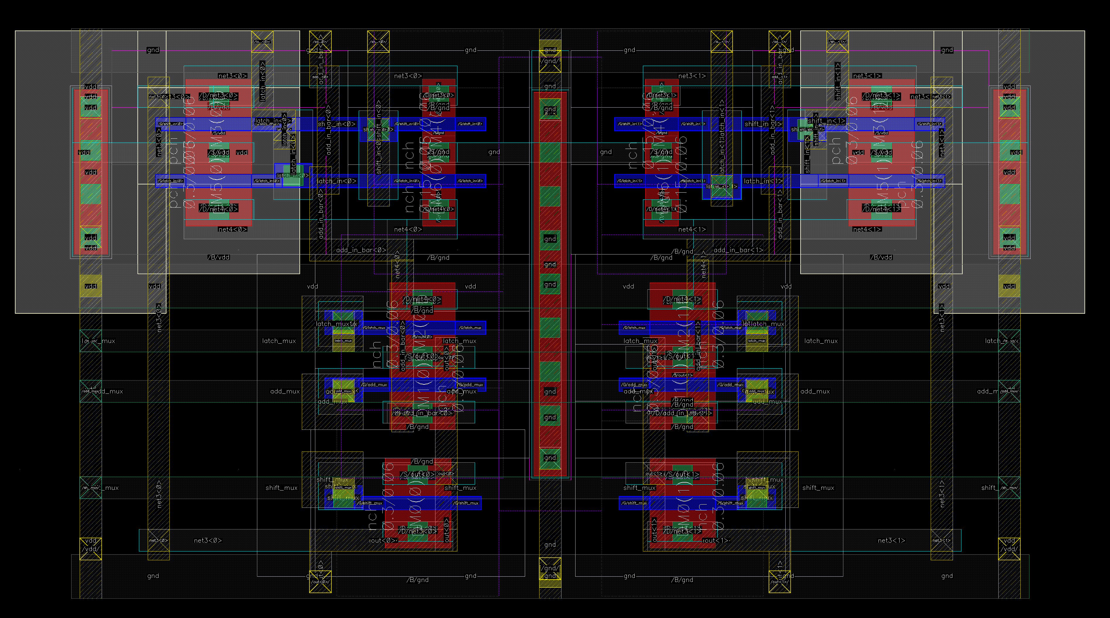
Let’s focus on a single-bit data block on the right.
M2: Connecting the Interface
Let’s start by connecting the shifter and the adder
At you see, if the M2 interfaces are misaligned, future routing will be painful, but still more than possible.
- Create a schematic.
- Instantiate the shifter and the adder. Align their power pins
- Move them closer, until you hit a critical DRC spacing violation
- NW/PP/NP spacing doesn’t count (you can fill that)
- The limiting factor is typically M1 or Poly
- If both blocks have an M3 power grid, you can try to align them
- Fix any DRC errors.
- Connect power rails at M2 level, if not already
- Connect the signal wires:
out<i>from the shifter should go inA<i>of the adder - Check DRC and LVS again. Make sure nothing’s shorted
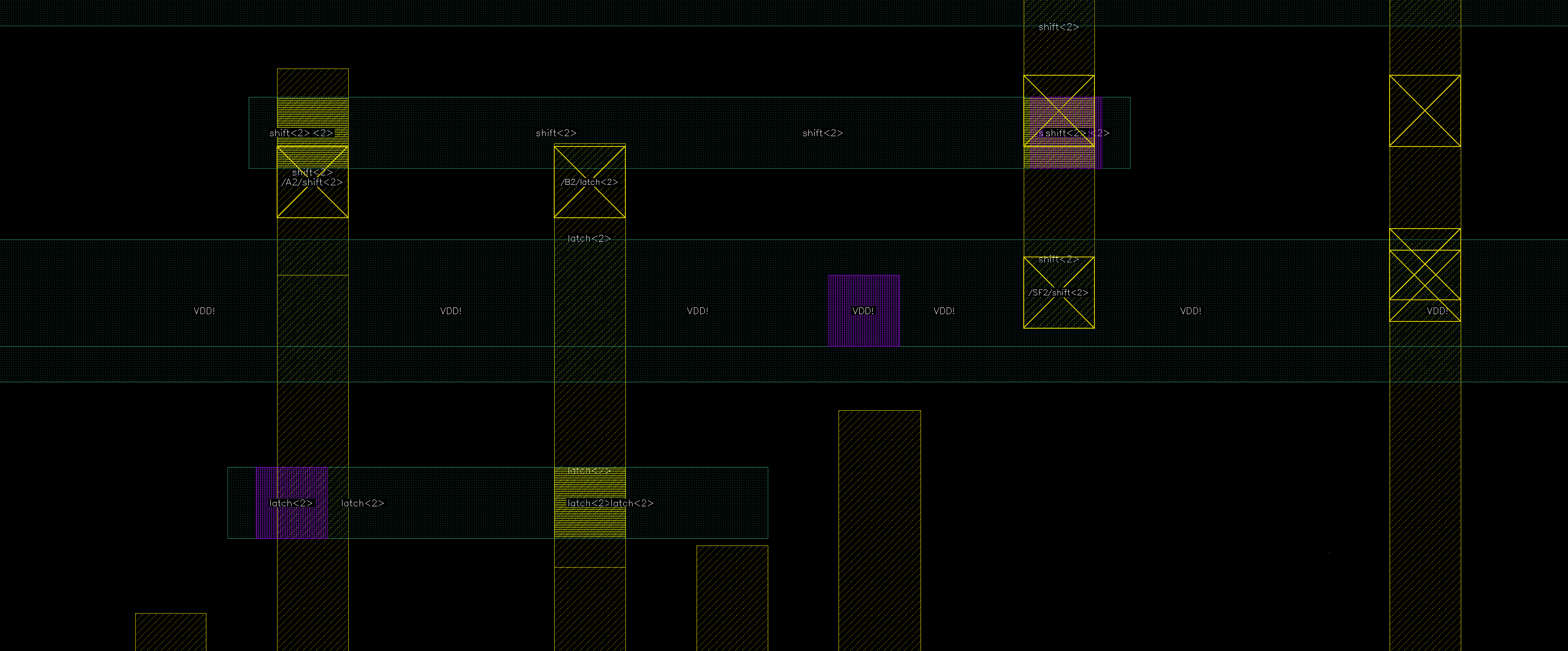
Above was our connection at M2. We didn’t design the adder and shifter interfaces to be fully compatible, so we need to make some tweaks:
- The
out<2>-A<2>path is misaligned, but no worries, we can temporarily route it to M3.- A cleaner fix would be to shorten the
B<2>pin in the adder.
- A cleaner fix would be to shorten the
- The
B<2>input comes from the top latch. I laid an M2 connecting theB<2>pin, and send it through M3 to M4 for the long-distancelatch<2>signal.
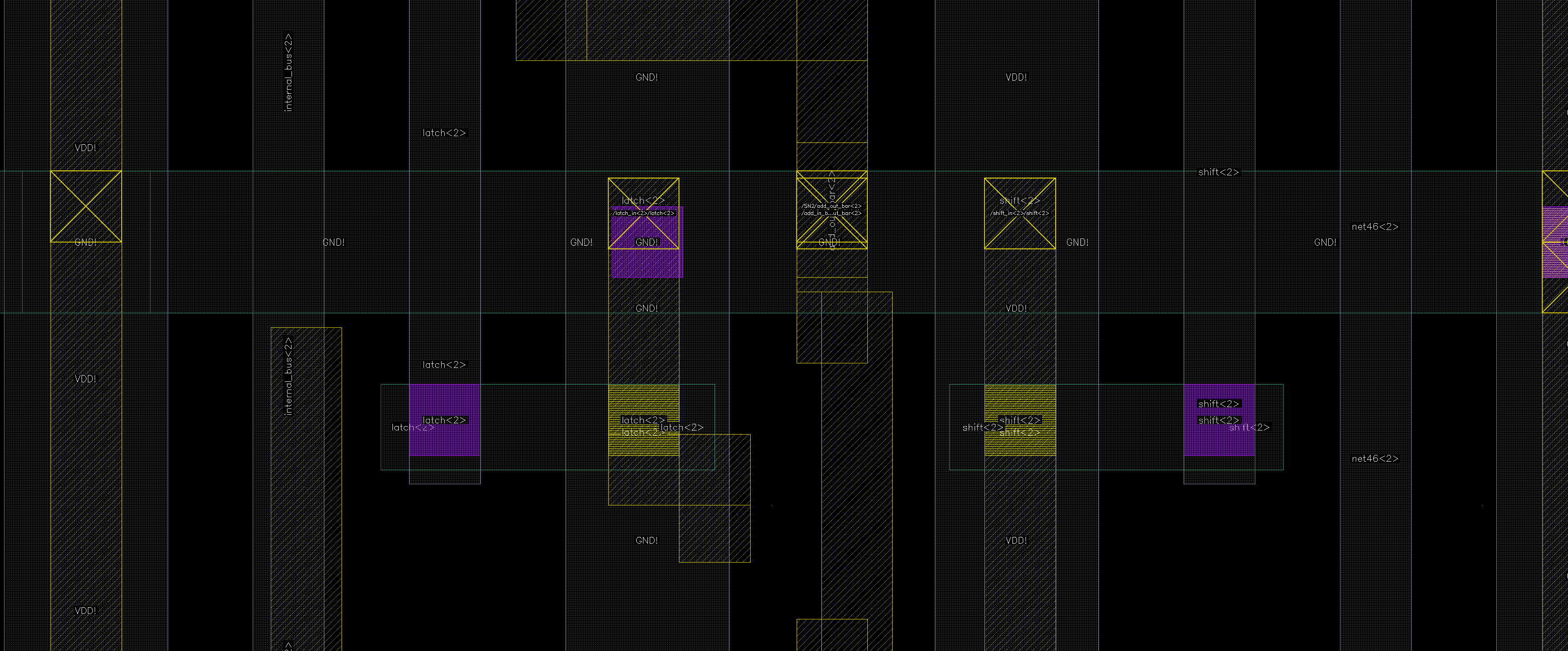
M4: Long-Distance Data
Your data wires should all fit within/above the data blocks. They should not significantly occupy any outside space.
Long-distance data routing at M2 is unrealistic. These should typically go to M4.
At M4, we have a much cleaner and spacious grid. We were even able to add an extra pair of power straps.
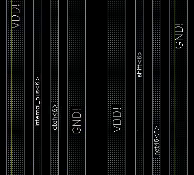
Above are the M4 wires at the adder block, where data wires are the densest.
I really don’t like the M4 color. It makes parallel wires look like the Twin Towers…
Let’s knock out the rest of the data blocks. You are a layout master rn. Just make sure you handle the inversions correctly
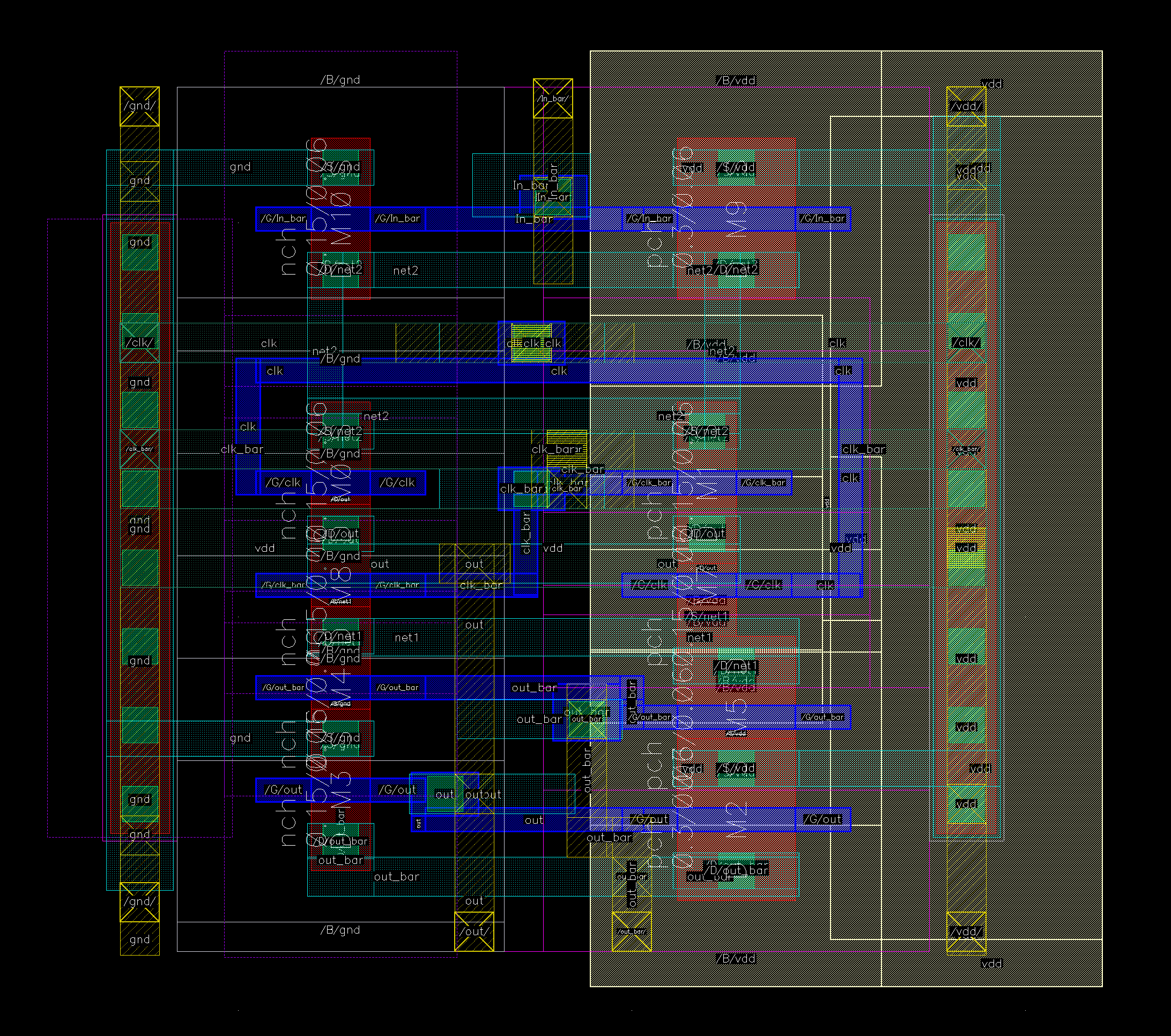
Latch
Same schematic as hw5.
MUX
We used a one-hot encoding for the inputs, making decoding much simpler on the MUX end
We used an NMOS-only gate, since the inputs are buffered; The outputs go immediately to the latch, which is also buffered.
Here is another example of connecting the adder and the MUX. The two other inputs are Viaed from M4.
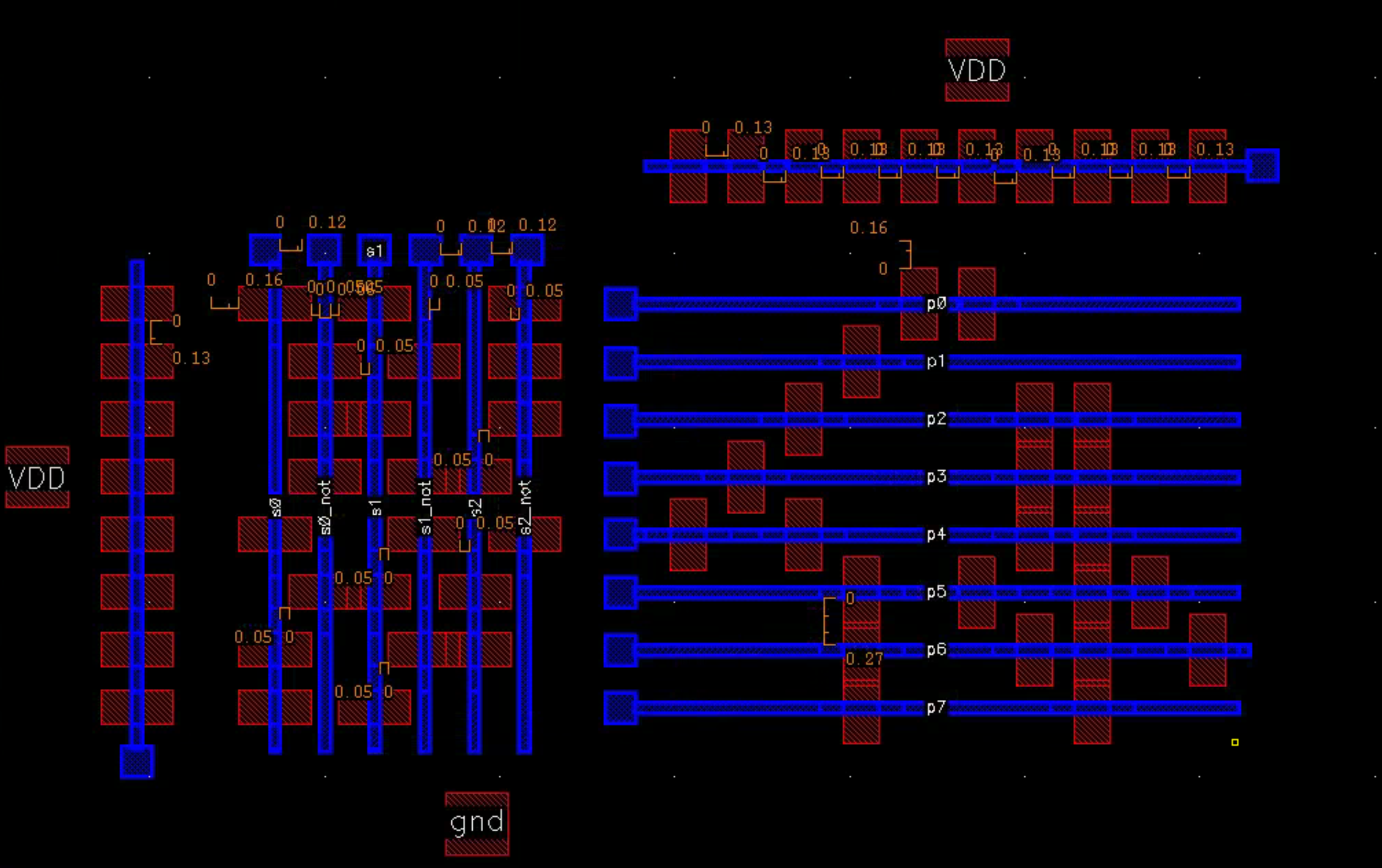
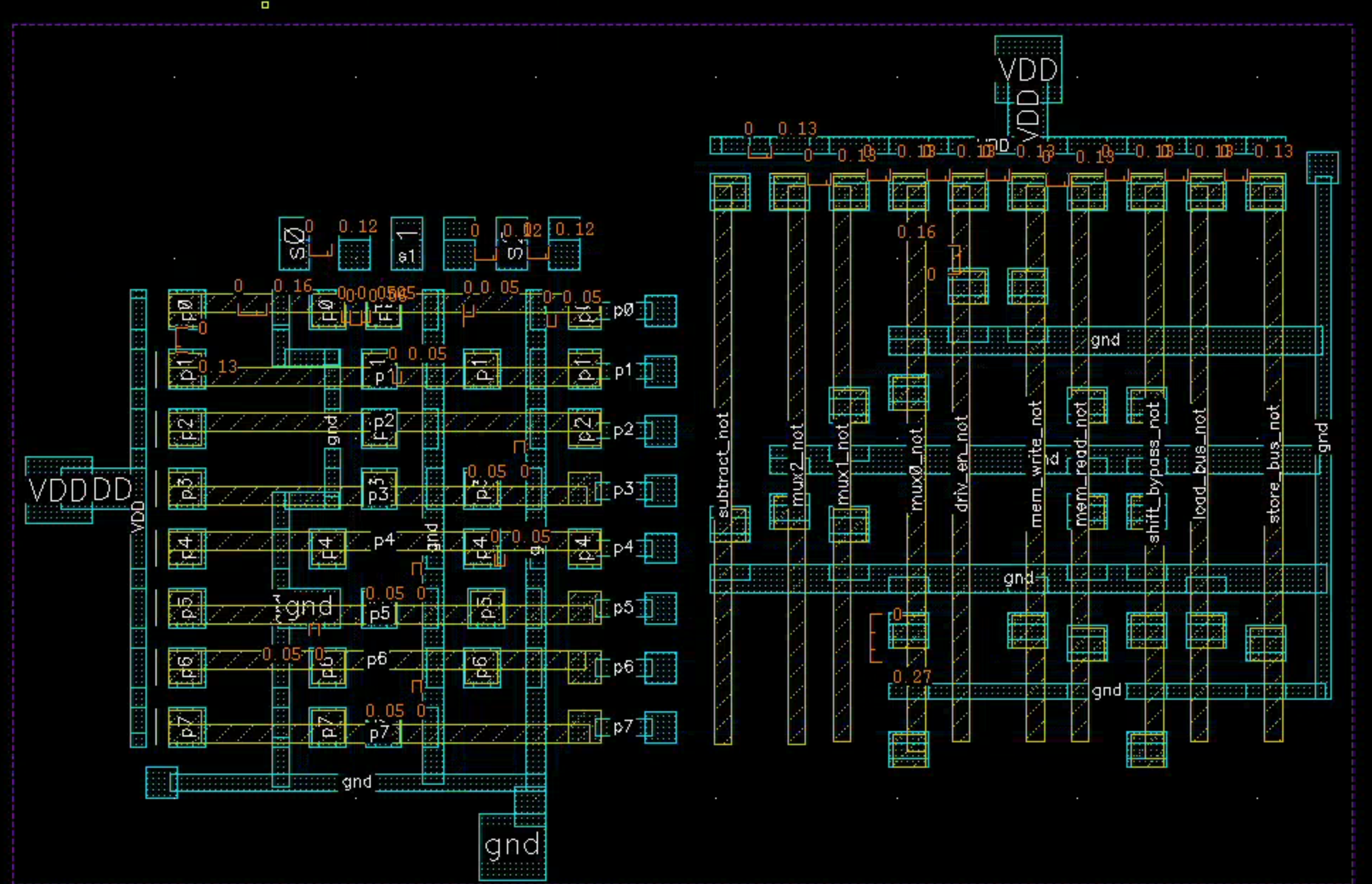
Bus Driver
Same as the SRAM bus driver, except to not skew the inverter 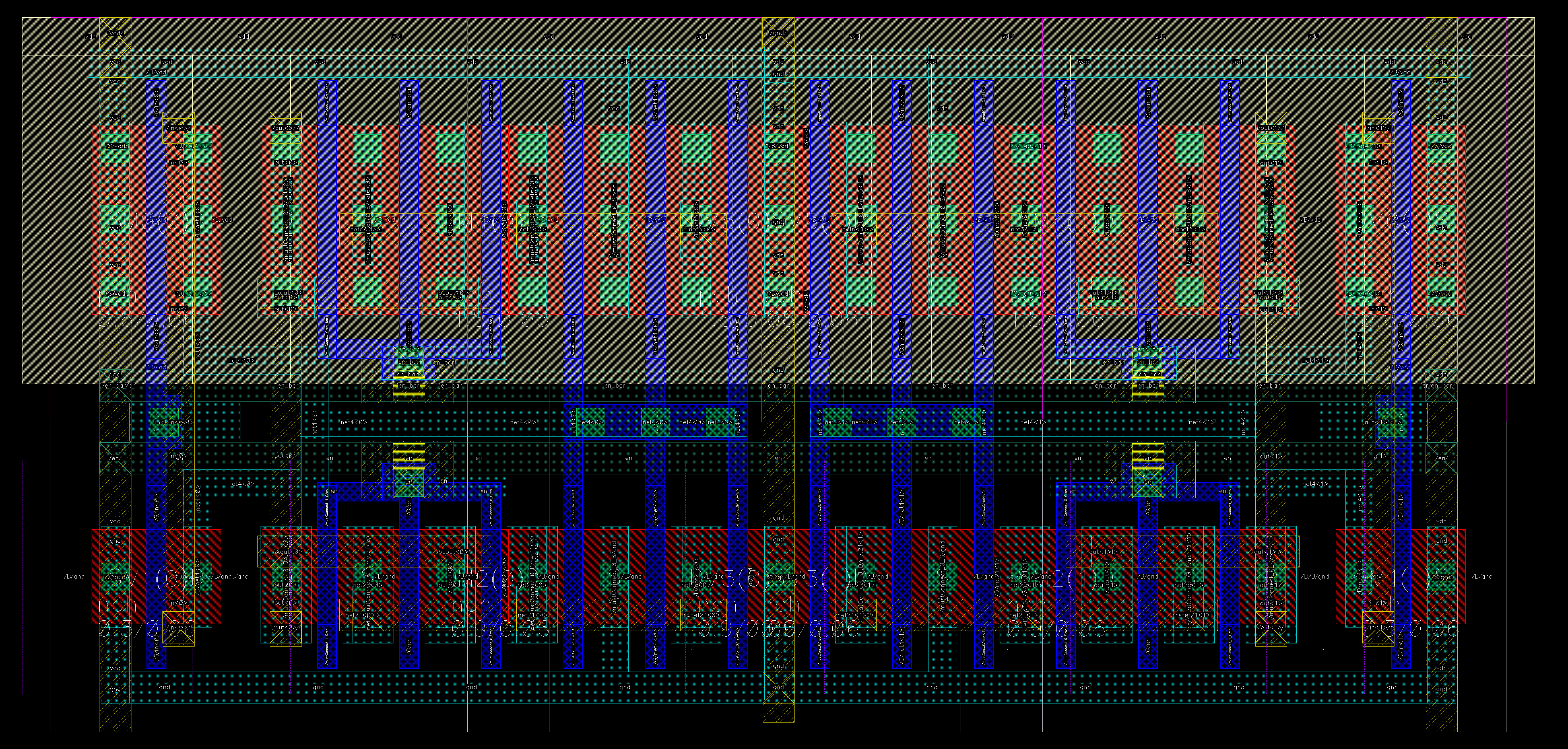
PLA
It’s not hard to lay out a PLA, but it’s hard to lay it well.
Planning
Before you start your PLA, have a clear floorplan of the entire processor.
Ask yourself:
- What control signals are needed from the PLA?
- What are their formats (binary encoded? One-hot?)
- Do they require inversion?
- Do they need additional downstream logic? Can I optimize those?
- Based on my data blocks, where shall I physically place the PLA?
- At which orientation?
- Do I need to adjust my existing grid?
- Based on the PLA placement, how should I roughly route the wires?
- How should I physically order the input/output wires to minimize routing effort?
- Do they need to cross the PLA? On which layer?
Schematic from Espresso
We chose one-hot MUX control (one extra output, but simplicity in internal logic)
Make a table of the logical outputs:
| Opcode | Assembly | Description | Internal bus driven by | MUX | Action |
|---|---|---|---|---|---|
| 000 | NOP | Hold Acc | – | Hold | No change |
| 001 | LOAD | Mem[i] ← External bus | external bus | hold | Memory write |
| 010 | STORE | External bus ← Mem[i] | SRAM | hold | Memory read; Drive external bus |
| 011 | GET | Acc ← Mem[i] | SRAM | Memory | Memory read |
| 100 | PUT | Mem[i] ← Acc | Acc | Hold | Memory write |
| 101 | ADD | Acc ← Acc + Mem[i] | SRAM | Adder | Memory read; Bypass shifter |
| 110 | SUB | Acc ← Acc - Mem[i] | SRAM | Adder | Memory read; Bypass shifter |
| 111 | SHIFT | Left logical shift of Acc | – | Shifter | Don’t bypass |
- Convert this to actual logic signals. Be precise.
- Inactive blocks must not modify state (E. in
Acc) - For actual don’t-cares:
- Use
X: simplify PLA logic - Turn it off: saves power
- Use
As you will see from the Espresso output, because the opcode space is fully encoded (3 opcodes → 8 bytes), Espresso can’t do much.
- Inactive blocks must not modify state (E. in
- Make a schematic from your Espresso logic. Start with minimum sizing for both NMOS and the pullup PMOS
- This consumes a lot of static power, though. You may want to use non-minimum length.
- Test your PLA schematic under all input vectors, and see if the output is expected
Stick Diagram
The textbook explains it on page 539.
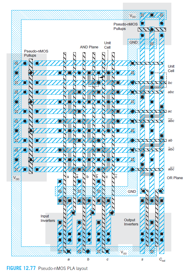
Start with one standard cell and push DRC limits. The rest follow naturally
- I recommend extracting the PLA and test its functionality and delay. Make sure all outputs are expected
Layout by William Wang
I would like to thank William Wang ’27 and his team for generously sharing their PLA layout. Their implementation closely follows the textbook design and achieves really impressive density!
Their diffusion sharing in the AND-plane was fascinating. While they use long poly, the circuit is so small that RC is less of a concern.
Our Layout
We tried to mitigate the RC Poly delay by laying parallel higher-level Metal and Viaing down to Poly gates, effectively breaking the long Poly segments. However, the Via stacks led to a larger design and spacing.
To fit the chip, we eventually rotated the PLA by 90°, completely disrupting the power grid (think Central Park in Manhattan). Highly suboptimal. Use the William design if possible.
Both designs draw significant static power. Consider using non-minimum PMOS length to trade area for power.
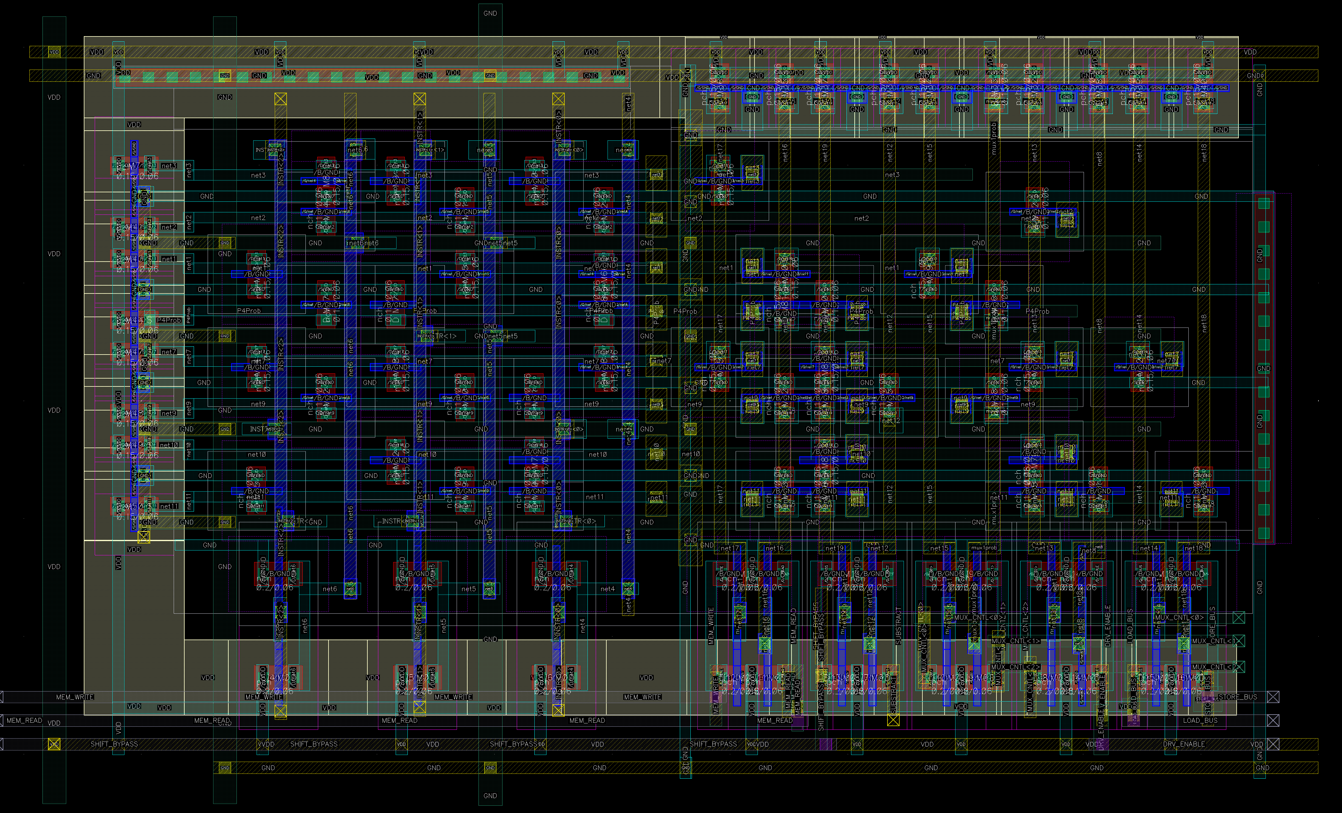
Control Path
You’ve gained enough “vibe-layout” experience from the SRAM. You don’t need an optimal solution– just one that fits and works
Reserve M4 tracks for the following:
- Clock
- Instructions
- Other long-distance/critical control nets
Latched Signals
The control signals to the adder/shifter need to be latched by phi_1. We implemented this by instantiating our single-bit latches and place them in parallel with existing latch blocks.
Shift Bypass
Two ways:
- Add a MUX in front of the shifter
- Qualify the
shamtsignal withshift_bypass_bar.
We chose the latter one.
DRC and LVS Tips
- DRC is quite straightforward. Run it early and often.
- LVS is one of the few nonlinear parts of this project. It behaves well when a small number of nets are problematic, and degrades rapidly once errors accumulate and propagate.
You may encounter “Incorrect Instances” or “Parameter Mismatch”. They are almost never sizing errors. Instead a short makes LVS to reinterpret the circuit topology
- Devices that should be separated are seen as merged
- Series/parallel devices are collapsed
- Netlist mismatch at device level
Large-net shorts (power, clock, buses) are especially problematic: When this happens, the error report typically explodes, and LVS was unable to localize the fault
- Try intentionally breaking the net and re-run LVS. Use divide-and-conquer to localize the short
- Pay special attention to overlapping Vias
Opens are less scary, as they usually produce localized error
Your extracted simulation should behave normally, given that you followed all the principles listed above.
Wrap Up!
CONGRATS on finishing most of the project! Give yourself a break, and get ready for this final push!
If your datapath looks good, your control path probably doesn’t (relatively). Let’s hide the sins.
Decap
- Use NMOS with a large width and length, but not too large (> 2 um, so \(r_o\) starts to matter)
- Put the NMOS in strong inversion (gate = VDD, others = GND)
Schematic Trick
Your probably need multiple decaps transistors in parallel:
- Create a
decapsymbol, which will contain all decaps. - Instantiate an
nch. Adjust with, length, fingers, and multipliers to fit in your largest dead area.- It would be really good if the decap contacts fit your power grid
- In the layout, “Update All From Source”. Share the diffusion and gates!
- Tune the sizes, if needed
You are probably very tired rn. Don’t chase perfection. Sufficient is enough.
Below are for aesthetics only
Pins
Extend your I/O metals to the boundary of your chip. Make pretty pins
Fig Leaf (遮羞布)
The rest of the circuit is what I call “遮羞布”. These dead areas come from the messy geometry of the control path, and instead of thoughtfully filling them with decaps, you inevitably give up and hide them under N-well.
Look how the irregularities are hidden!

Final Check
FIN