
4321 Inverter
Published:
Take a read of Shepard’s Online CAD Tutorial. It’s very comprehensive guide.
- Below, we’ll walk through the process systematically and highlight common pitfalls so you can avoid a massive learning curve.
- If anothing messes up, see if it’s in the Virtuoso FAQ
Layout
Assuming you have already designed and tested the inverter schematic
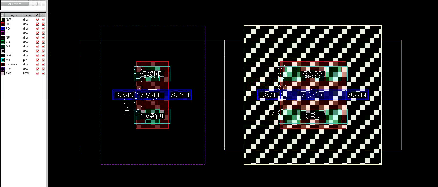
1. Generate All From Source
- In Virtuoso, create a new “Layout” with the same name as your schematic
- Use “Connectivity/Generate/All From Source”. It will generate the two transistors, and a few cyan (M1) Pins
- The instances between schematic and layout should match. Selecting one highlights the other.
- Rotate the transistors by 90 degrees.
- Align the transistors
- Make sure
NPandPPboundaries perfectly align. No gaps or overlaps
- Make sure
Layers
Before drawing, it’s important to understand each layer in Virtuoso:
On the sidebar, you can double click on a layer to make it exclusively visible, and inspect each layer individually
MOSFET
A MOSFET is a piece of silicon with 4 terminals: Gate, Source, Drain, and Body. S and D are typically symmetrical.
Body
NW(N-Well): PMOS bodySUB(P-Well, SUBstrate): NMOS body- Marked by
PDK
- Marked by
Source/Drain (diffusion)
OD(Oxide Diffusion): source and drainPP(P imPlant mask,pimp)PP∩OD: p+ diffusion
NP(N imPlant mask)NP∩OD: n+ diffusion
Gate
PO(POlysillicon)
Metal
Silicon/metal interface
CO(COntact, Ohmic): connectsPO/OD(silicon) withM1(metal)M1: First Metal layerVIA1: connectsM1andM2M2: Second Metal layerVIA2: connectsM2andM3- and so on…
Pin
Used to label connections across hierarchies. Nothing electrical.
If you are interested in the physical implementation of these layers, this article explains in glorious detail
2. Body Vias
Next, we need to connect the Bodies to the power supplies. Click o to add M1-SUB and M1-NW Vias.
- Again, make sure
NPandPPboundaries between the transistors and vias perfectly overlap.
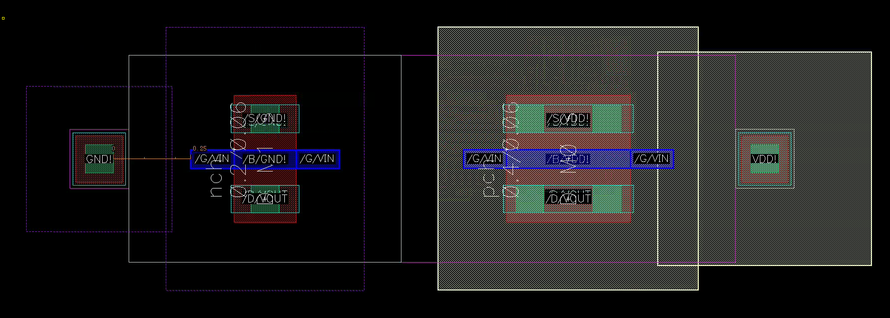
The Vias have a similar stack of 5 layers connecting Body to Metal:
NW(P) / substrate (N)NP(P) /PP(N)ODCOM1
The “Detached Body” option creates Body contacts explicitly. Not needed if you’ve used Body Vias already.
A Body Via can power a large region of P/N substrate. You don’t have to use a Body Via for every transistor. (~30 um)
3. Connections
Now, use the rectangle tool (r) to connect the PO gate and M1 source/drain to complete the circuit: 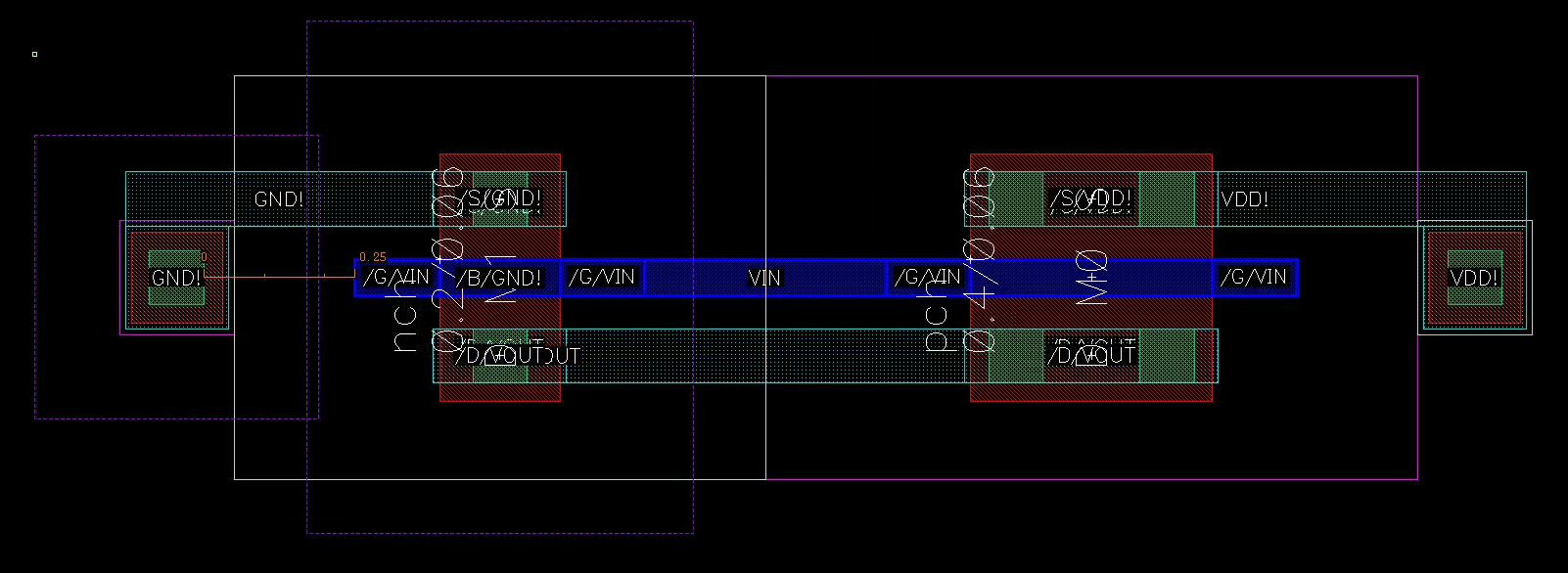
You are allowed to overlap the rectangles. Only their union counts.
DRC
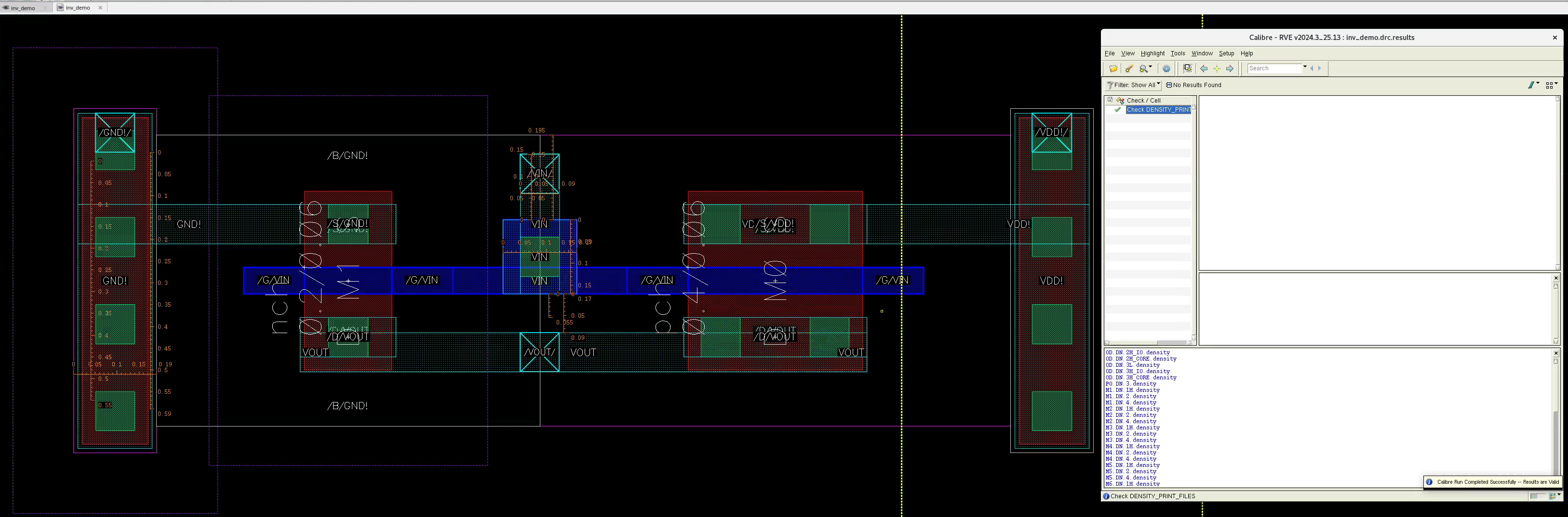
Run DRC as frequently as possible, especially if you are a beginner!!
Skip to Shepard’s Calibre DRC tutorial and set up the environment
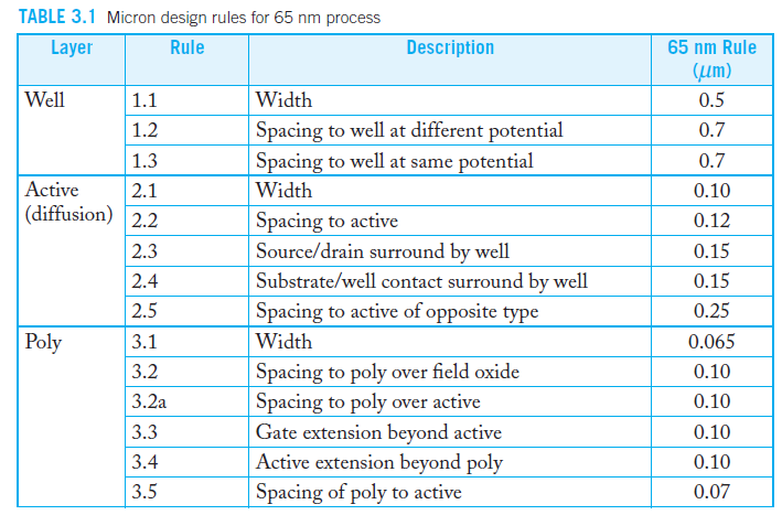
Below are the main types of DRC errors for TSMC N65:
- Shape rules
- Shapes must satisfy a minimum area
- Shapes must have a minimum width
- Shapes must also meet constraints, such as a minimum side length
- Inter-shape rules
- Enclosure: for example, a Via must be properly enclosed by its associated Metal layers
- Sometimes, minimum overlap or enclosure area also apply.
- Spacing: minimum spacing must be maintained
- between shapes of the same layer, and
- between shapes on different layers, such as spacing to body connections
- Enclosure: for example, a Via must be properly enclosed by its associated Metal layers
Here’s a (simplified) list from textbook pages 118-119
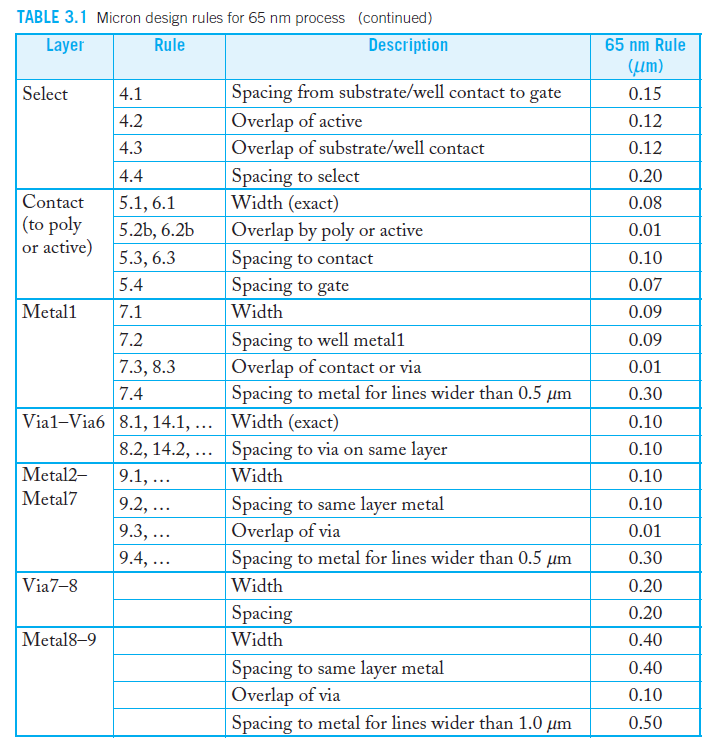
Let’s run a DRC right now: 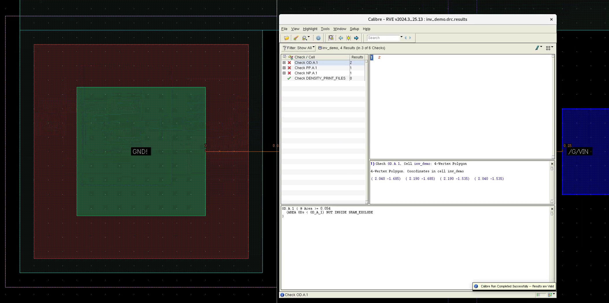
RIP, got 4 errors. They are because the OD and PP/NP areas of our Body Vias are too small. Since we have ample space, we can simply make them larger. You can:
- Increase the number of rows/columns of the Vias
- This is simple. 4 rows/cols will work
- Manually draw a larger
OD/PP/NParound the current layer- This is more risky, as changing one layer may violate other spacing/enclosure rules,
- but useful for aggressive optimizations, as you will see later
We are now DRC clean!
4. Gate Via
There’s one more step to connect the gate input. Add a M1-PO via.
Similar to the Body Vias, this M1-PO also has the following layers PO, CO, and M1. All layers must satisfy DRC rules.
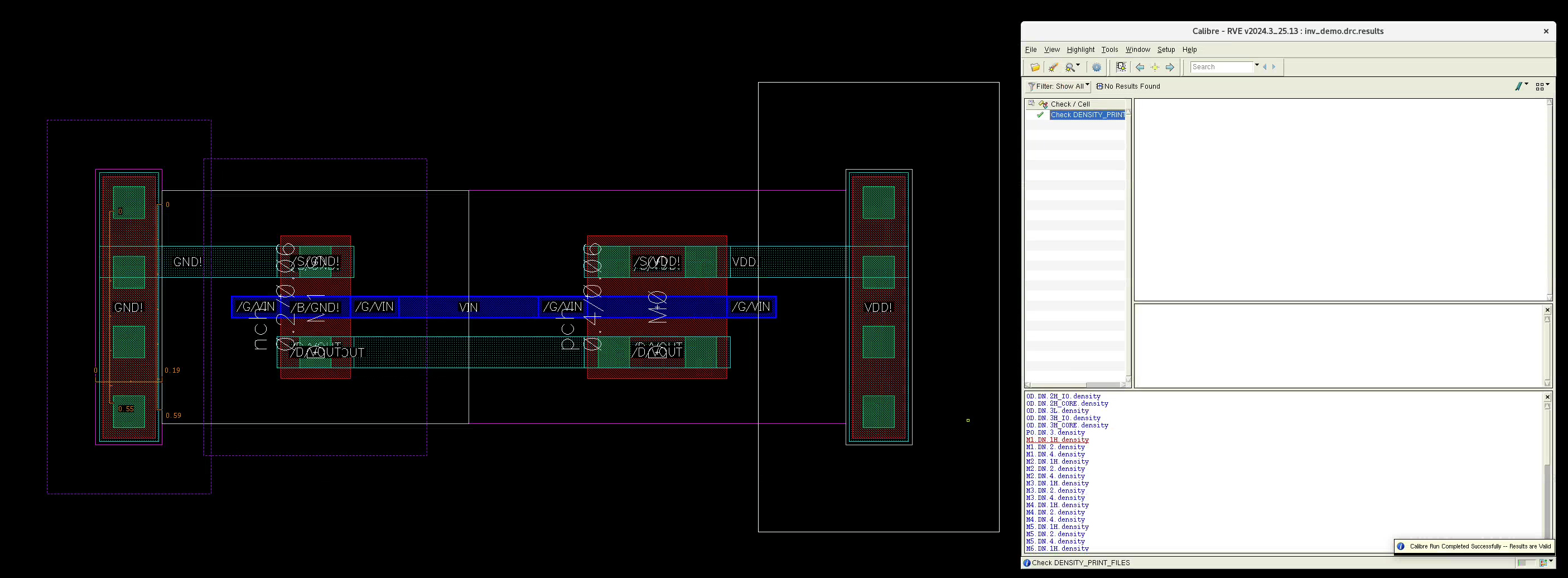
Now run a DRC:
RIP, another two violations. Make only M1 layer visible for more clarity
M1of the via is too close with our VOUTM1.- Fix: Move either
M1rectangle away, so that they are at least 0.09 um apart
- Fix: Move either
M1of the via’s area is too small. It’s like an island- Fix: Add a larger
M1rectangle to the via so its area is more than 0.042 um²
- Fix: Add a larger
LVS
Use m to move the Generated M1 Pins over to the metals.
Check LVS. Read the tutorial for the setup
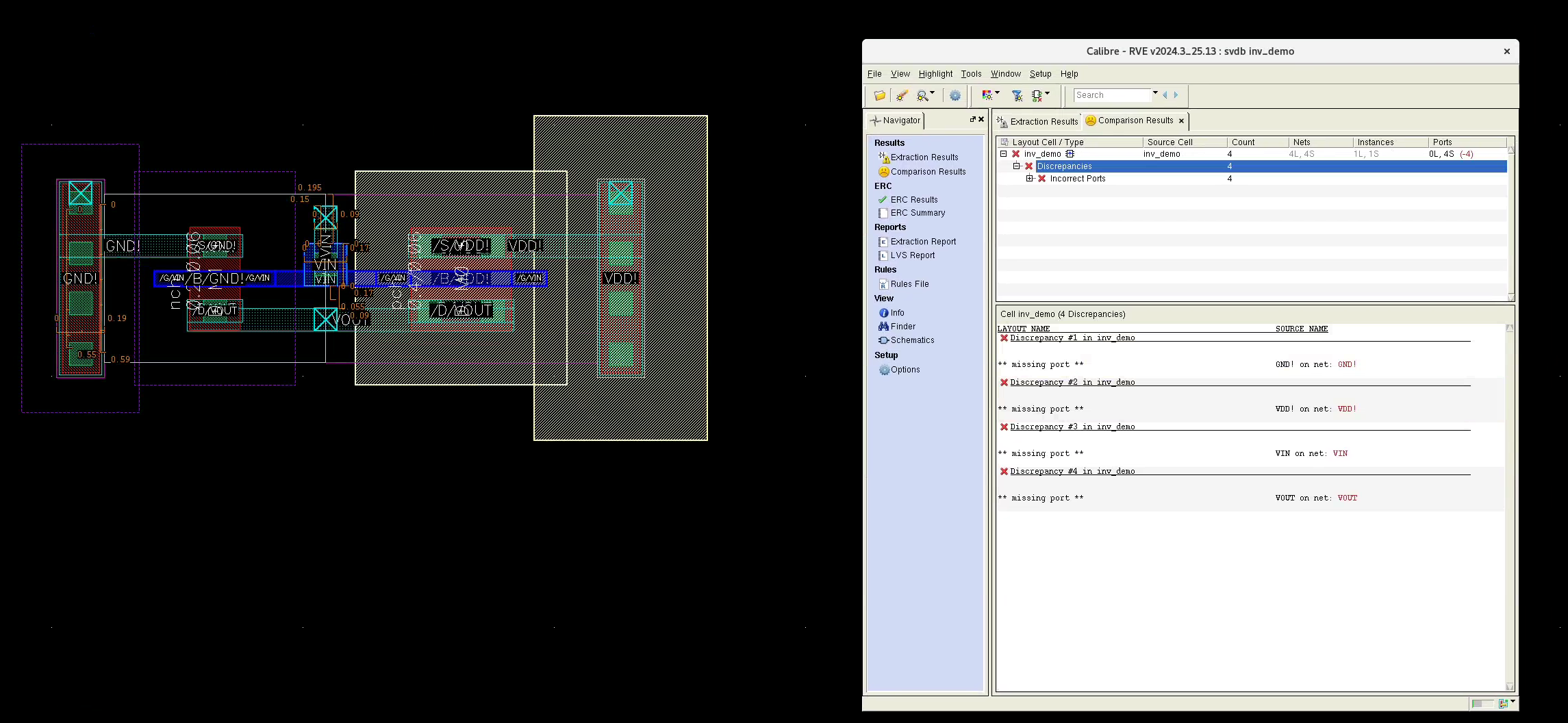
If your layout is LVS clean, skip this part
RIP, we got 4 “Incorrect Ports” errors. Calibre LVS somehow does not recognize our pins, despite that they are created with labels! This is very rare…
In this case, first check if Virtuoso recognizes the pin. Try moving the pins around and see if the label (“VOUT”) and the cross shows up. If not, delete the pins and do “Connectivity/Update/All from Source” again. Make sure you select the “Create Label” option
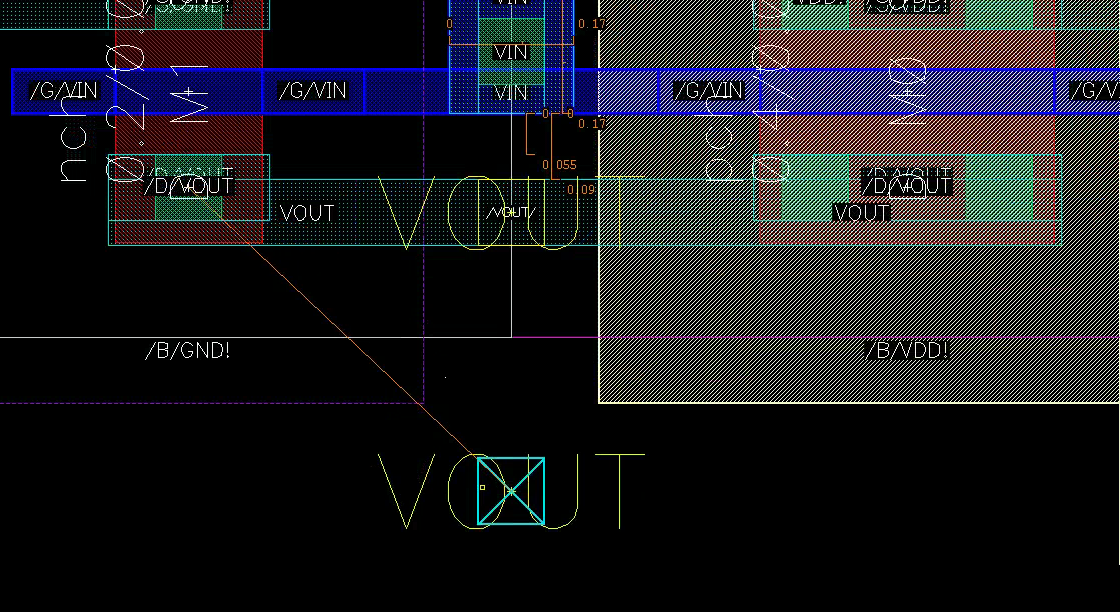
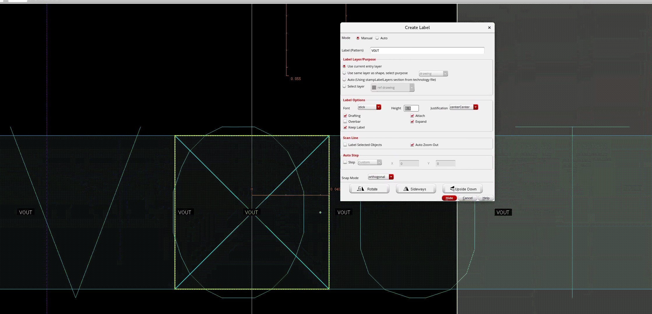
Here, Virtuoso does have the label, so let’s manually add the labels to the pins again to let Calibre LVS know.
- Click
land create label “VOUT”. - Click the center of your pin
- Choose “Purpose”: “pin” as the object
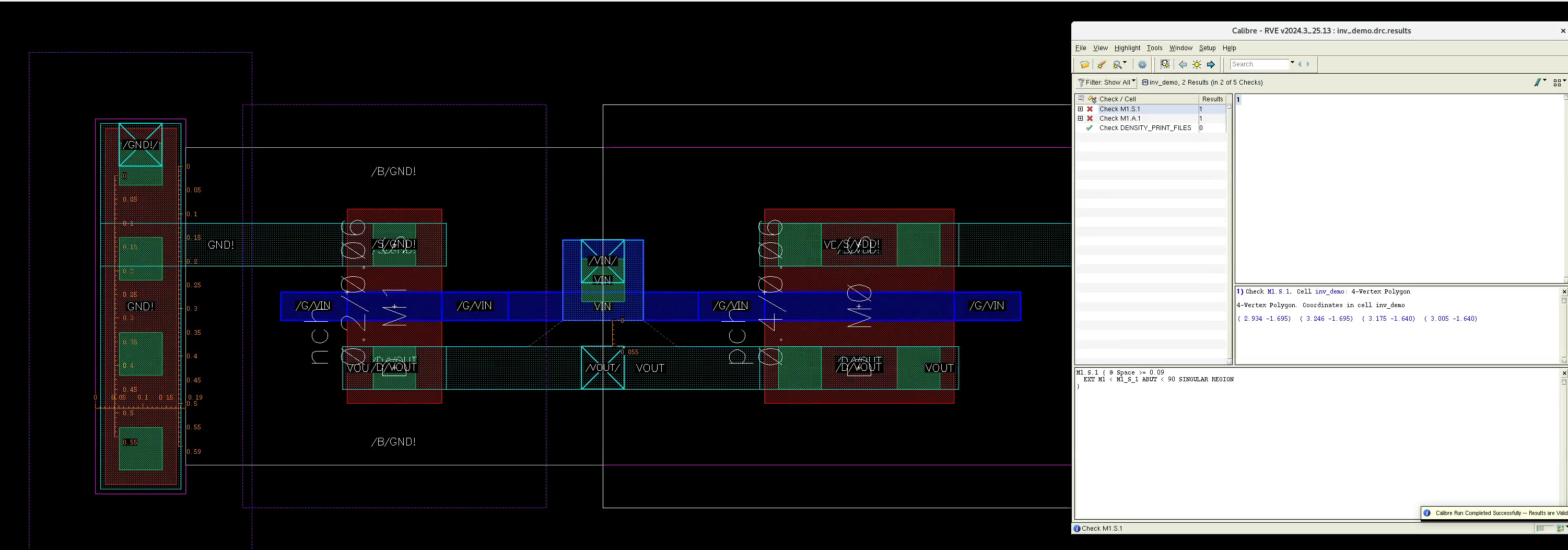
Now, as a proof of concept, run LVS again to see if the error count drops to 3:
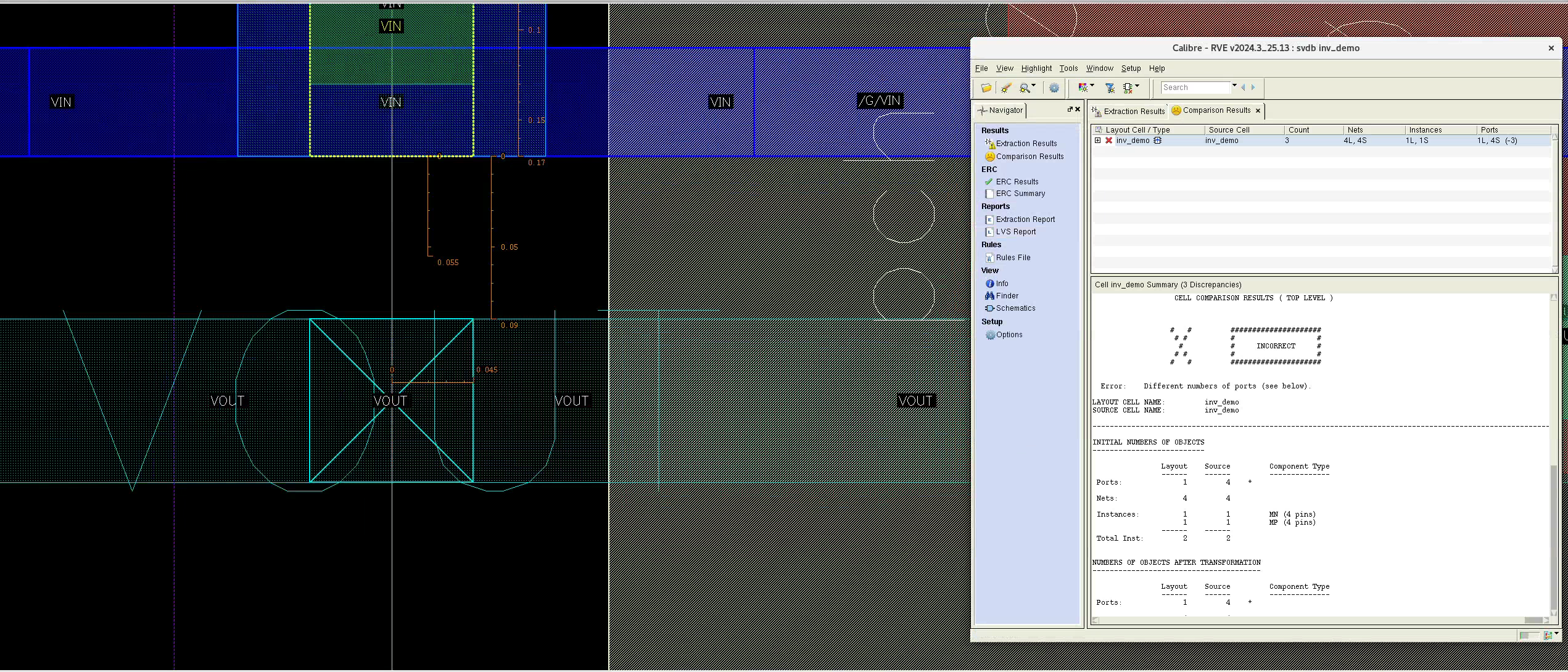
Yep, so add labels to the other three, and you will be LVS clean!
Virtuoso FAQ
When I open Virtuoso, all my instances show up as red boxes
Click Shift+F to display instances, and Ctrl+F to hide them
My pins do not have labels on them (or LVS doesn’t recognize them)
In the “I/O Pins” tab of “Connectivity/Generate/All From Source”, you have to set “Pin Label/Create Label As/Label”. Set:
- “Font Height”: 0.1 (recommended)
- “Layer Name”: “Same As Pin”
- “Layer Purpose”: “Same As Pin”
Cadence keyboard shortcuts stopped responding
Stacked functions. If you accidentally repeat commands before previous ones have cleanly finished, it may mess up Virtuoso’s stack, blocking the UI. In this case, close unused tabs, and press ESC to quit current functions
My layout nets are not showing up
Open with Layout XL