
1-Memory
Published:
DRAM
Dynamic Random Access Memory: address -> data Content addressable memory: key -> address (Unit 3)
On PCB, DRAM packaged in DIM (Dual Inline Memory Module)
- Usually 8 chips (9-10 if error correction)
- Connected to CPU/SOC using the DDR (dual data rate) bus
- DDR: data can be transferred at both clock edges (double frequency)
- GDDR: graphics
- LDDR: low-power
- DDR5: latest standard
- Data bus width: 64 bits (32x2)
- Address bus: 21 bits (Longer addresses take multiple cycles; slow if too wide)
- Command bus: 7 bits (?)
- 64 ms refresh
- DDR Standard: JEDEC, allow different manufactures to interoperate
- In SOC, the Memory Controller controls the DRAM
- May have more than 1 MCs
- Each MC can be attached to more than one DRAM modules
- The connection DDR is a channel
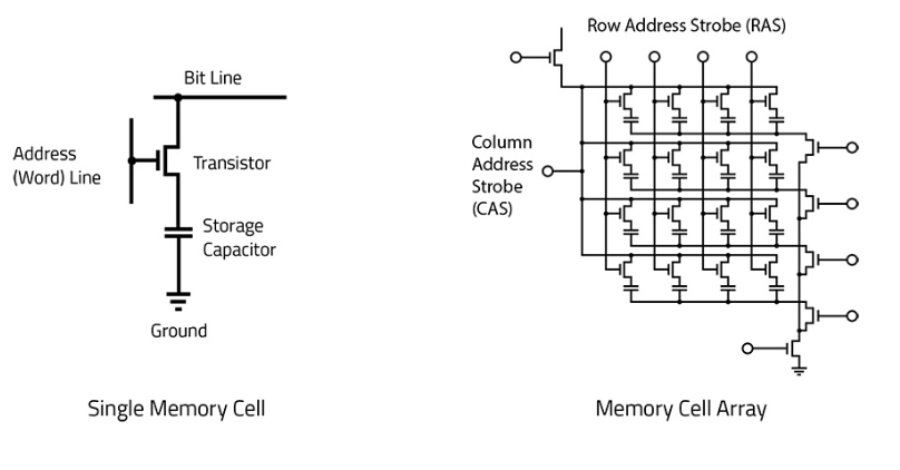
DRAM Cell
G: word line; D: bit line
Write:
- Activate word line
- bit line = value
Read:
- Activate word line,
- Discharge value = bit line -> Analog sense amplifier (amplifies to drive)
- Take output, and restore the value
Subarray
aka “mats”, square to normalize latency
- Bit line connected to sense amplifiers
- Address -> decoder -> word line cell -> subarray -> mat -> sub-bank (~4) -> bank -> chip -> rank -> channel -> DIMM
Bank groups (BG0-7) on a DRAM die
Page buffer in one bank: sense amplifier that holds a data row
- Each row can be as wide as 8K
- Refreshing can happen concurrently (other banks can be refreshed while one is read)
- Any command from processor is broadcasted to all dies
E. DRAM bus runs at 2400 MHz. What is the peak bandwidth between the memory and the SoC?
- 2400 * 2 * 8 bytes (maximum)
Don’t forget to x2
64-bit: 8 byte per transfer
Commands
REFRESH
- \(t_{REFI}\): maximum supported refresh interval (~4000 ns)
- Limits the peak BW
- \(t_{REFC}\): blocking time for refresh per row (~200 ns)
- E. about 95% BW available
READ
ACT(activate row): drop all data to the bottom buffer on the bank- Energizes a particular wordline for subsequent access
- \(t_{RCD}\) (row-to-column delay) from
ACTtoCAS
CAS(column select)- \(t_{CL}\) (column-read delay) for data to be read out
- Data bursted out then (bursted out in group of 16 (burst length))
PRE(precharge): so the nextACTcan happen- Precharges the row to \(\frac {V_{DD}} 2\) to drive the sense amplifier
- \(t_{RAS}\) (row-access strobe delay) between
PREto the nextACT - If reading a different row in the same bank, \(t_{RP}\) (row-precharge)
- Not necessary if reading the same row
Error
Soft Error Prone to particle strikes (E. \(\alpha\)), may trigger bit flips
- Want detect and recover
- Store data redundantly (E. 2x to detect, 3x to correct)
- ECC (E. 2D parity)
Hard Error DIM-SOC bus line stuck at 0 all the time
Failure model
FIT: failure of 1 GiB of memory per 1 billion hours of operation
- ~15 for memory
- ~100 for GPU memory
SECDED: correct 1-bit faults, detect 2-bit faults
- Typically done in 64-bit chunks Chip kill: make sure still works if one chip in DIMM fails
Correction Scheme
TMR (Triple Modular Redundancy): give 3 copies to have a majority vote
- Very cumbersome (3x load latency + comparison; 1/3 capacity)
- Can correct any number of bit faults
Error Correction Code
- Sometimes black box
- Support errors in the check bits
- Data \(d\) (E. 64 bits) + check code (E. 16 bits)
- Multiply \(d\) by a constant \(m\). Store \(dm\) in memory
- When retrieving, divide by \(m\). If no remainder, good;
- If there’s a remainder \(r\), we know which bit to flip
where \(k\) is the position of the bit flip To correct,
\[\frac{d'}m = \frac{d\times m}{m}\pm \frac{2^k}m\]Need to find \(m\) such that \(\frac{2^k}m\) produces unique remainder for all \(k\) (E. 243)
- Constraint on \(m\): minimize the number of check bits
- For double error detection, you get a remainder that matches nothing
Error Correction Scrubs (ECS)
Error accumulate over time so you can’t correct
- Solution: scrub memory periodically
- Error correction happens in the memory controller: Need to read + write from the chip
- Also a blocking operation
DDR5 only does SEC (no double-bit) (Q: is it required on thei chip, or ???)
Random Access Strobe timing
\[t_{RAS} = t_{RCD} + t_{CL} + t_{RP}\]E. DDR5 memory, 1 DIMM on the system, 8 GiB, no ECC, clock 3000 MHz. Estimate the latency of 2 successive (back-to-back) reads to two different rows in the same bank
- 8 chips on the DIMM, each with 8 Gib of memory; to output 64 bits of data
- \[t_{RCD} + t_{CL}*n + t_{RP} + t_{RCD} + t_{CL}*n\]
- Multiple \(t_{CL}\)s that reads burst of data
- No need for last recharge E2. Same condition, but to the same row
- \[t_{RCD} + t_{CL}*n + t_{CCD} + t_{CL} * n\]
- No need \(t_{RP}\) twice
- \(t_{CCD}\): column-to-column delay E3. Two different banks E4. Two different DIMMs
- …
Cache
Speed limited by memory
- Even worst due to instruction fetching (same time as memory access)
- Store these locally within the SoC in faster memory -> cache
SRAM
Bistable element, with charging capacitor on each side
- On die
- Same process technology for memory as with CPU
- Planar CMOS, trench capacitor
Hierarchy
- CPU
- L1I, L1D (L1I -> CPU -> L1D pipeline)
- L2
- L3
Main memory Each layer has ~10x capacity & access time
- Temporal locality: loop
- Spatial locality: array
Physical organization
2D array
- Line (block) size: 64B
- x # of cache lines Address -> decoder -> tag array -> data array
When caching address, tag address = x « $log_2$(cache line size)
Associativity
- Direct mapped: one addresses only map to one index
- Set associative: one address maps to a set of indices (aka ways). May be in either of it. Decoder checks if either tag in the ways
- If hit, extract address offset
Policy
Evict policy
- Random
- Least recently used item (LRU)
- Most recently used item (MRU)
- OPT: relying on a oracle knowledge
- Adaptive (based on ML algorithms)
Store policy
Hit
- Write-back: only update L1, mark line dirty
- Write-thru; Update propagate to higher levels (L2, L3, …)
- Simple coherence
- Slow Miss
- Write allocate: bring data to cache and write
- Useful for
calloc() - Good temporal locality
- Works well with writeback
- Useful for
- Write around: skip level you miss. Update the level where data hits
- Useful if no further reuse (E. logging, stream media,
free())
- Useful if no further reuse (E. logging, stream media,
Between levels miss (level specific):
- Inclusive cache: $level_x \subseteq level_{x+1}$. Store in all intermediate level
- Exclusive cache: a cache line exists uniquely in one level.
- aka victim caching (evict to next level)
- NINE: neither, no commitment, in-between
MSHR
Performance optimizations for loads
LD x
LD x+4
LD x+8
LD x+12
Suppose x misses in L1D. Cache Controller issues to L2
- While L2 is accessing
x, processor looks forx+4- Wasteful here to issue another miss for
x+4 - Processor fold subsequent misses to the same pending cache line This is called MSHR (Miss Status Handling Registers). Tracks all pending misses
- Wasteful here to issue another miss for
- Table of missed addresses, corresponding to PC of all subsequent loads
- One table for each level of cache
HW Table has limited size of the number of addresses, and the number of PCs for each address.
- If no space, stall CPU (no folding available)
Write Buffer
Performance optimization for store misses
st x
st x+4
...
Buffer up the stores in a write buffer (mini cache with addresses and 1 line data)
- Once filled, evicts and sends to the next level. If you load the same address as stored, data forward directly from buffer
Example
Q: How many lookups happen in L2, and how many writes go to the DRAM? L1D MSHR: 4 entries
miss[3:0], each can handle 16 misses Suppose load 32K ofints, 64B cache line size
- First miss instance is stored in a cache line
- Subsequent misses on the same line are buffered (folded)
- For L2 layer, need 32K / (4 * 16) = 512 cache line lookups
- Without MSHR, 64x more
- 16 * 4 due to 16 fold * 4 bytes for
int
- Exact same as L1D line size, since
intis the most common- Every 16 misses are collapses into one L2 lookup
L1D store buffer: can combine consecutive writes to 1 cache line
Suppose store 16K
ints, 64B cache line size
- If L1D store miss, send to L2, but not individually
- Write buffer collects every write into a single cache line
st c[15:0](forint)- When line filled, send the request to L2 to write
- Without store buffer, L2 4096 writes * 4 byte
- With store buffer, LL2 4096 / 16 = 256 writes * 64 bytes
- Same data, but less metadata (location, write size, etc.)
- In L2, still write allocate system -> all misses -> send to DRAM
- No additional merging possible. All misses are cache line size
- If you alternate cache writes,
st c[i]; st d[i], store buffer will be useless due to conflict
DRAM traffic
- Memory Controller (MC) that receives all miss traffic from SoC. Makes request (
PRE,ACT, column R/W) to DRAMAssume
- 16 GiB DIMM
- 8 Bank groups (each DRAM is x8, also sending 8 bits of data)
- Each BG has a row buffer
- 8 open rows per DRAM
- 64 open rows per DIMM
- 4 sub-banks per bank group
- 2 subchannels per DIMM
- Miss traffic trace
- Assume no code misses. Data only
- Reason from L2 output
read A[0:15]
read B[0:15]
// still stuck here, but processor will keep requesting
// non-blocking write
read A[16:31]
read B[16:31]
write C[0:15]
Q: How should PA -> DRAM address mapping be set up to improve parallelism
- Make sure
A,B,Cneed to be written to different banks concurrently
- If same bank, blocking each other. Won’t need to issue separate open and close
- E. BG0 has slice of
A, BG1 has sliceB- When MC controlling cache line requests into DRAM commands, process out of order
- Readings are more critical. Make it happen before the write
- Instruction page > read > write
- aka memory scheduling
Cache causality
Reason of misses:
- Cold (compulsory): first reference
- Capacity: too small (even if fully associative)
- Conflict: addresses map to the same cache line
- Assume cache is infinitely large and fully associative
- Any miss will be cold -> label them
- Solution: pre-load all data into cache (prefetch)
- Hardware prefetcher (ML-based)
- Also increase block size
- Finite capacity, FA
- Misses: cold + capacity
- Solution: increase capacity
- Finite capacity, SA/DM
- Will have everything
- Subtract the previous two out -> conflict misses
- Solution: increase associativity
- change cache indexing (hashing function)
- change replacement policy
- Capacity -> latency
- Block size -> latency (but less extent)
- Associativity -> latency
Fully associative structure
CAM: content associative memory
- (tag, data) pairs
- Search the tag in parallel in every row. If match, data out.
- Typically 1 clock cycle
- Number of items searched in 1 cycle: search scope of a scan
- XNOR check every bit of the tag -> every bit ANDed
- The key bits are broadcasted to every cell -> latency increases very rapidly
PORT
How many R/W can do to a given memory at a time
- E. 1R1W; 1RW; 2R1W
- 1RW: standard SRAM array. Only one address (wordline) you can energize
- 2R: additional wordline and bitlines attached to every cell. Two sets of sense amplifiers. To transistors controlling the read -> more latency
Example:
- RF: 2nR, nW (n is the number of concurrent instructions in-flight)
- L1: 2R, 1W
- L2: 1RW
HW1
clflush(ra): evict from cache block. If cache line is 64 bytes, need to do for allra % 64rdtsc: timer, issued before and after- Need to serialize the instructions
- Use
rdtscp - Or insert
cpuidjust before therdtsc lfence
mfence: prevent multiple CPU cores to interact with memory at the same time Noise reduction techniques:- Pin process to specific cores:
taskset - Pin certain page for DRAM:
mlock
Virtual Memory
Very large linear array, abstraction. Allow portable code
- 0 to \(2^N-1\).
- The next location is previous location + 1
- Not all physically addressable
Caching
How to provide such VM illusion Physical memory = populated DRAM (~GB) + size of swap space (E. SSD, HDD, tape ~TB) Solution: cache VM chunks into physical memory Raises a few questions
- Block size? page size (OS page size, not to be confused with DRAM row buffer size)
- In modern OS, 4 kB, 1 MB, 2 MB, 1 GB
- Associativity? fully associative
- When
malloc()called, a chunk is allocated and mapped to the DRAM page- Allocates anonymous data. Not stored to hard drive
- After certain
malloc()s, DRAM fill out. Moved to swap space - If swap space also fills up: Out Of Memory (OOM). Can no longer illusion
- For file-backed data reading, resides on non-volatile storage
- Placed in DRAM page cache when read
- If miss in DRAM, swap space fetch cost is very expensive. Associativity reduced conflict misses.
- Search is done in software (OS)
- Can’t do FA for lower-level cache, since hardware algorithms for searching data can’t execute in ns.
- When
- Eviction policy?
- Store hit policy? exclusive between swap space and DRAM
- Except page cache in DRAM is inclusive (caches hard drive files)
- Flush command pushes page cache to hard drive
- For anonymous data, DRAM is the final destination
- Except page cache in DRAM is inclusive (caches hard drive files)
- Store miss policy? write allocated to DRAM
This is called software managed cache
- Replacement in SW (higher latency)
- Fully associative
Page Table
Data and metadata (ana tag)
- Page address
- Permission (rwx)
- WC (does it support multiple consecutive writes)
- UC (uncacheable)
- User/kernel Need to know which pages are present in DRAM + Swap
Data structure: page table Need to
- Locate item quickly (E. n-ary tree)
- allocate/deallocate pages
- Small in size
Page walk
aka search through the tree for address translation
- Implemented in HW or SW
E. if tree has 5 levels, need 5 reads to get a memory address.
TLB
Cache page walks -> Translation Lookaside Buffer
- Special cache for VA -> PA pairs
- Same level as L1
- One page walk done, cached to TLB
VM cannot be directly mapped to cache, since different programs will have different VA. Need to first translate to PA
- Can directly translate if sure that PA not used by any other addresses Program -> VA -> PA (page walk, TLB cached, else expensive) -> cache
- TLB latency + cache latency
- 50% overhead :(
VIPT
Optimization: given VA, lookup in TLB and cache concurrently
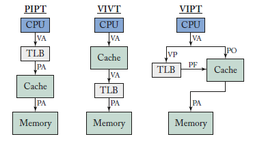
VIPT caches (Virtually Indexed Physically Tagged)
- Virtual address to compute index
- Physical address to check tag
- Need VA -> PA to conserve index & offset bits
- \(log_2\)(page size) = index + offset bits
Translation overhead
- PA only: embedded system
- If you know exactly how many processes the system has.
- No dynamism
- Page table
- High radix structure (tree) to optimize the search
- 4-5x overhead!
- Cache VA -> PA translation in TLB
- Virtual page number -> physical page number
- Only pay cost once
- TLB is fully associative, since misses are very expensive
- VIPT: hide TLB lookup latency under cache latency
Virtual page number cache index cache offset
Optimizations
Cache size limited by page offset bits. Suboptimal Solution: make cache set associative, so each index can store multiple tags
- Allows larger total cache size for same index bits
- If TLB miss, raise an exception (TLB fault), handled by OS or hardware microcode
- Page walk, and fill in TLB
- Build HW caches for each page walk level (again)
- Known as MMU caches
- If no translation exists (first-time access): page fault
Example
Virtual -> physical -> cache -> DRAM
int *a = malloc(4096 * sizeof(int));  // dynamically allocated
// same for b and c
c[i] = a[i] + b[i];
Suppose 64-bit VA space, 40-bit PA space -> $2^{40}$ max DRAM capacity
- OS page size: 4 KiB
Max page
- Max working set size (data only) = 3 * 4096 * 4B= 48 KiB -> 12 page table entries
malloc()will align to page entries.aligncompiler command
Physical Config
Suppose:
- L1D: 64 k, 64 B lines x 64 sets x 16 ways
- L2D: 256 KiB, 64 B lines x 16k
- L3: 8 MiB, 64 B lines
- Writeback for hit, write around for miss
- 4 KiB page size
- VIPT
Q: What is the size of the L1D tag array, assuming a VIPT cache - Page size = 64B x 64 sets = 4K - 40-6-6=28 bits of tag (use physical size) for each line - Total: 28 bits * (64 sets * 16 ways)
- Assume a FA, 16-entry TLB
- TLB is 1 valid bit + VPN tag + PPN tag
- Size of one entry = 1 + (64-12) + (48-12) = 69 bits
- If TLB includes the bits used from MRU replacement,
- 4 bits of index for MRU entry, 4 more bits
- If include LRU replacement,
- 4 bits for each MRU entry, 16 more bits
- OR a matrix with comparison bits for each entry: 16 * 15 / 2
- More data, but simpler comparison algorithm
Code Optimization
To improve locality E. A 2D (byte) matrix is laid out linearly in memory
- Load The bae address
- Add offset (0)
- Store this address to somewhere else in memory With cache (E. 4-entry, FA cache, line size: 4B, writeback on store hit, write allocate on store miss)
Suppose transposing a matrix, row accesses will hit, but column ones will miss
- Memories are in row-major order, so the columns will miss!
- Change how arrays are accessed, and increase
- Fetch a square block of data into the cache -> Cache blocking
- Set up loop index, so the amount of data accessing fits into the cache size