Elmore Delay Analysis
Published:
Recitation 01: Elmore Delay Analysis
The 18-4/622 Staff
Recitation Notes, Fall 2026
(a) Gate Elmore Delay
The following problem was taken from the 18-4/622 F25 Midterm Exam
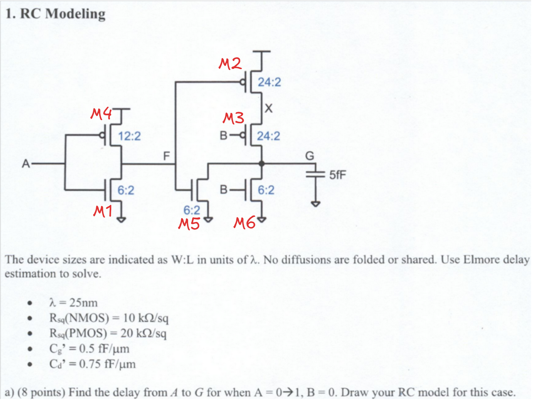
i. Identify the Switching Paths
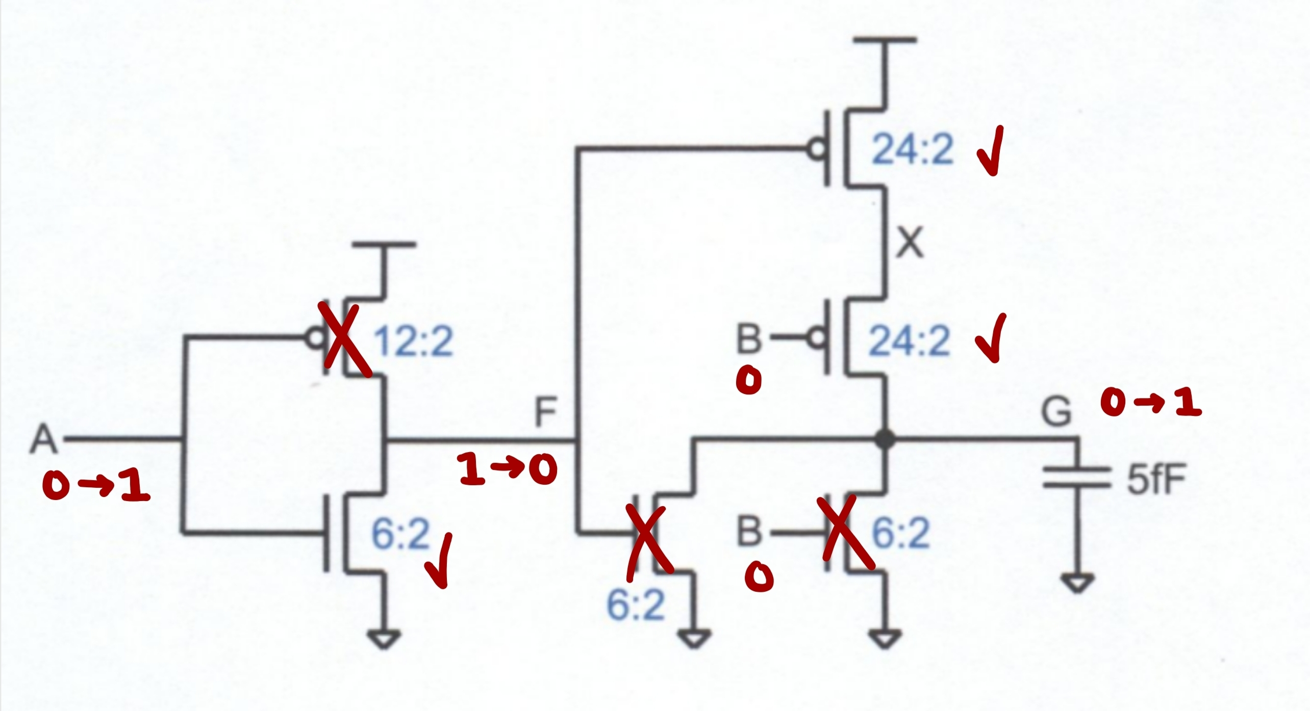
To calculate RC delay, we first identify which transistors are actively turned on during the switching event to form the charging and discharging paths:
- Initial state: A = 0, F = 1, B = 0, X = 0, G = 0
- After transition:
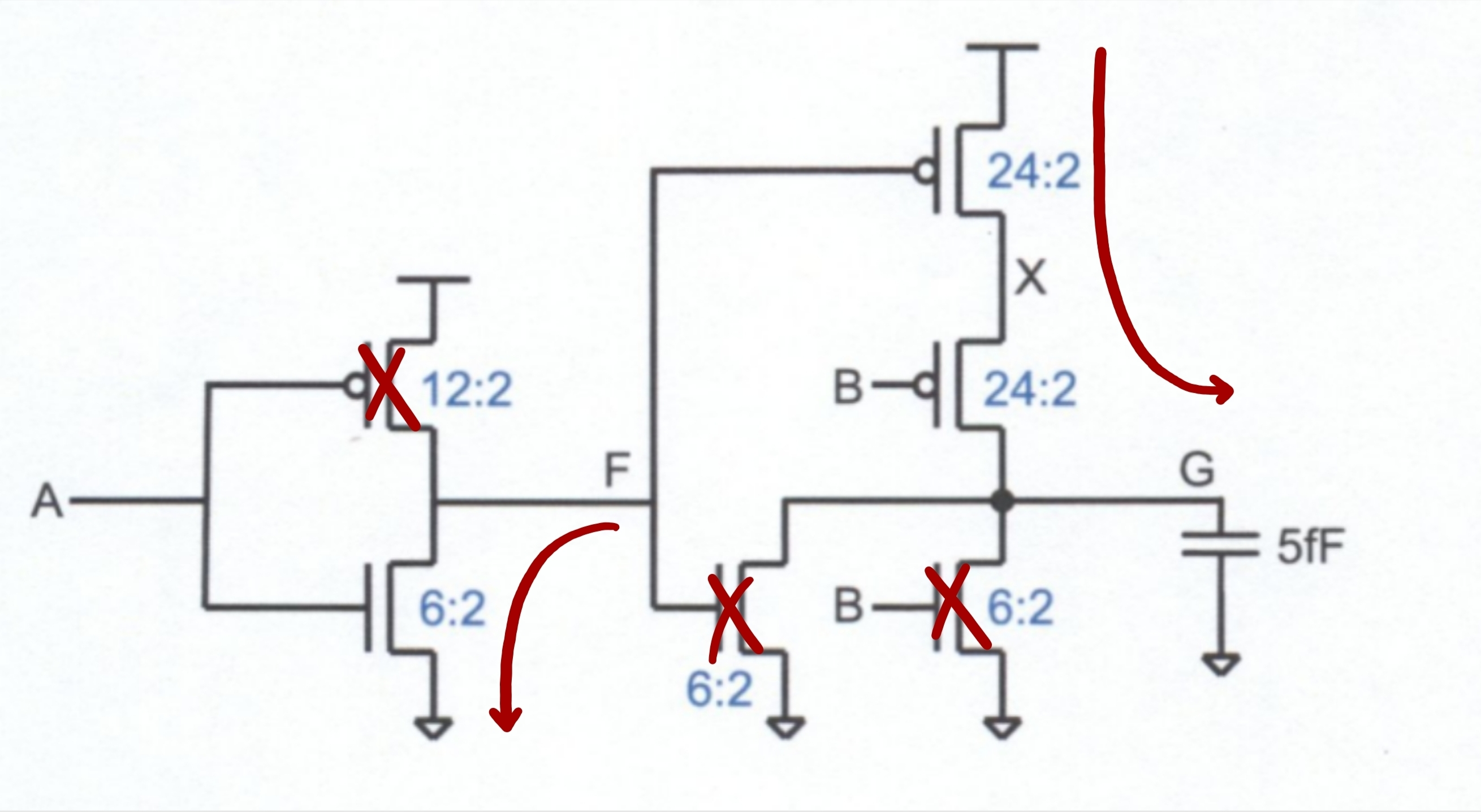
- A → 1, F → 0 pulls down to GND through M1
- X → 1 pulls up to VDD through M2
- G → 1 pulls up to VDD through M2 and M3
What if M2 and M3 inputs are swapped?
X = 1 throughout the transition. All parasitic caps at X will not draw switching current and will not be part of the delay
ii. Develop an RC Model
Recall the switched-RC model of a transistor: 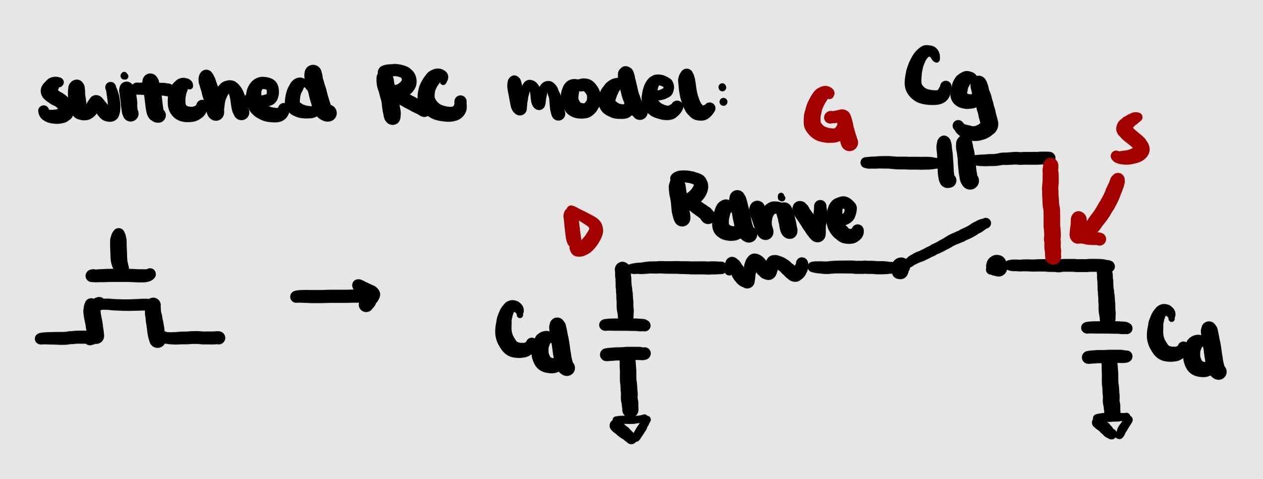
\(R_{drive}\) is the resistance of the semiconductor channel. In our digital model, we mainly consider two parasitic caps:
- Gate capacitance \(C_g\)
- Includes \(C_{gs}\), \(C_{gd}\), \(C_{gb}\). For digital estimation, assume \(C_g \approx C_{gs}\)
- Diffusion capacitance \(C_d\)
- Junction capacitance at the drain and source. Again, for our models, assume \(C_d \approx C_{db} \approx C_{sb}\)
Applying this transformation yields the complete switch-level RC network: 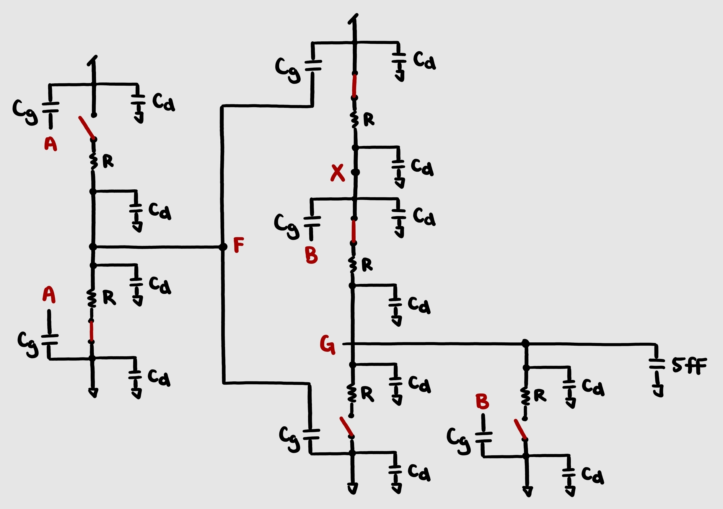
iii. Find and Compute Relevant RC Values
Resistance
As we observed earlier, the channel resistances of M1, M2, M3 form the resistive network in the RC delay model.
Channel resistance is calculated using the square resistance formula:
\[R = R_{sq}\frac{L}{W}\]- M1: \(R_1 = 10\,k\Omega/\square \cdot \frac{2}{6} = 3.33\,k\Omega\)
- M2: \(R_2 = 20\,k\Omega/\square \cdot \frac{2}{24} = 1.67\,k\Omega\)
- M3: \(R_3 = 20\,k\Omega/\square \cdot \frac{2}{24} = 1.67\,k\Omega\)
Capacitance
There’s a ton of caps here. Let’s collect them at each node, and add them in parallel. A few things to note:
- Supply-tied nodes are ignored: capacitors connected directly between supply rails with no series resistance do not contribute to switching delay, and can be removed from our models
- If a source node is floating rather than directly tied to a rail (M3), its parasitics \(C_{gs}\), \(C_{sb}\) will (dis)charge through the RC network and must be included
Cleaning up the diagram with these rules in mind: 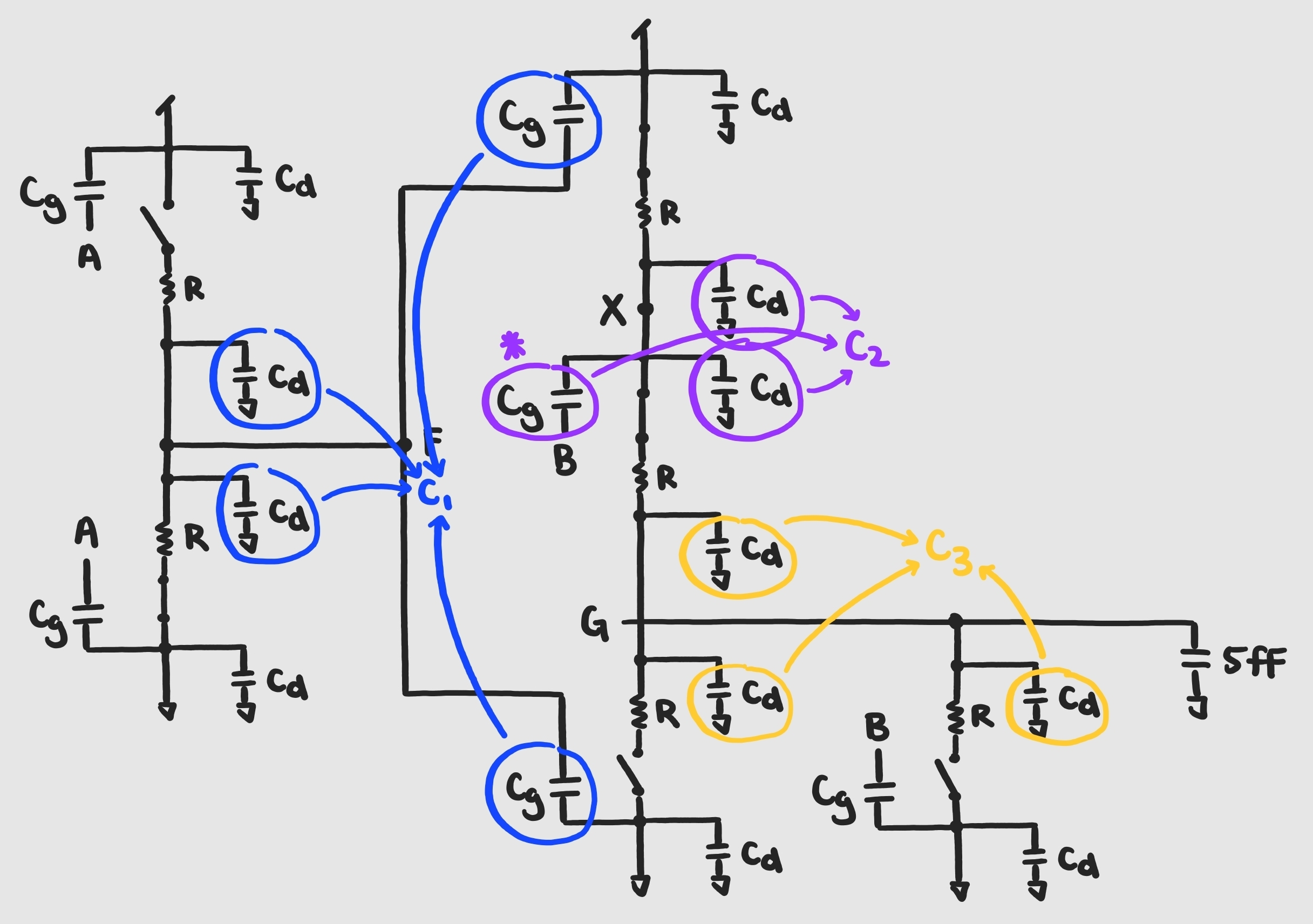
- Node F: \(C_1 = C_{db,M1} + C_{db,M4} + C_{gs,M2} + C_{gs,M5}\)
- Node X: \(C_2 = C_{db,M2} + C_{sb,M3} + \color{red}{C_{gs,M3}}\)
- Node G: \(C_3 = C_{db,M3} + C_{db,M5} + C_{db,M6}\)
Plug in the numbers:
- Node F: \(C_1 = 0.75\frac{fF}{\mu m}(6+12)(0.025\,\mu m) + 0.5\frac{fF}{\mu m}(24+6)(0.025\,\mu m) = 0.71\,fF\)
- Node X: \(C_2 = 0.75\frac{fF}{\mu m}(24+24)(0.025\,\mu m) + 0.5\frac{fF}{\mu m}(24)(0.025\,\mu m) = 1.2\,fF\)
- Node G: \(C_3 = 0.75\frac{fF}{\mu m}(24+6+6)(0.025\,\mu m) = 0.68\,fF\)
A practical shortcut
For any node with minimum channel length \(2\lambda\):
\(C_{node} = C'_g\left(\sum W_{gates} + \sum W_{floating\ sources}\right) + C'_d\left(\sum W_{diffusions}\right)\)
- Q: How would R and C scale when using non-minimum length channels?
iv. Compute the Elmore Delay
There are two ways to collect the RC terms. Take a moment to convince yourself that they are equivalent:
- For every resistor, multiply by the sum of all downstream capacitances drawing current through it
- For every capacitor, multiply by the sum of all upstream resistances shared along its path to the supply
Using the first method:
- A → F: \(D_1 = R_1C_1 = 2.38\,ps\)
- F → G: \(D_2 = R_2(C_2 + C_3 + C_L) + R_3(C_3 + C_L) = 20.92\,ps\)
And the total delay is
\[D = D_1 + D_2 = \boxed{23.29\,ps}\](b) Wire Elmore Delay
This wasn’t covered in recitation, but might make for some useful practice.
Q: If we insert a wire at node F with \(R_{wire} = 50\,\Omega\) and \(C_{wire} = 5\,fF\), what is the new delay? Use a single-segment pi model for the wire. Draw your RC models for this case.
The pi model splits the capacitance evenly on both ends. Inserting it into node F: 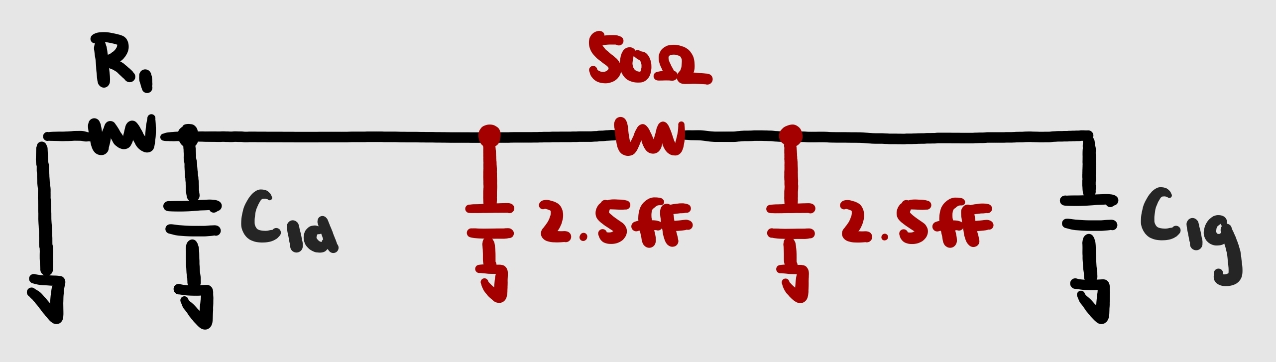
\(C_{1g}\) goes on the far end of the wire, while \(C_{1d}\) stays on the near end.
The modified delay is then straightforward:
\[\begin{aligned} D_1' &= R_1(C_{1d} + C_{1g} + C_{wire}) + R_{wire}\left(C_{1g} + \tfrac{1}{2}C_{wire}\right) \\ &= 3.33\,k\Omega\,(0.3375 + 0.375 + 5)\,fF + 0.05\,k\Omega\,(0.375 + 2.5)\,fF \\ &= 19.19\,ps \end{aligned}\]Let’s make sense of each term here:
| \(C_1\) | \(C_{wire}\) | |
|---|---|---|
| \(R_1\) | \(R_1(C_{1d} + C_{1g})\): original delay | \(R_1C_{wire}\): driver resistance charging the full wire cap |
| \(R_{wire}\) | \(R_{wire}C_{1g}\): wire resistance charging the far-end load cap | \(\frac{1}{2}R_{wire}C_{wire}\): wire intrinsic self-delay (pi model) |
Exercise
Rederive \(D_1'\) using a T-model, an L-model, and a 4-segment pi model. Which terms will change, and which terms stay the same?
\(D_2\), the delay between F and G, remains the same, so we get:
\[D' = D_1' + D_2 = 19.19\,ps + 20.92\,ps = \boxed{40.10\,ps}\]Congrats on surviving Problem 1 on the midterm!!
Don’t worry if it looks overwhelming at first! Once you digest the steps, you will do it fast and easy. In the end, the math is just multiplying \(RC\) in fancy ways and summing them up. You’ve got this!
– The 18-4/622 Staff