FFT Core
Published in Advanced Digital Design, Spring 2026, 2026
Design and VLSI Implementation of a high-performance, 1024-point Radix-2 DIF FFT core
Architecture
- 16-bit fixed-point precision
- Data SRAM, twiddle factor ROM
- TSMC 65 nm CMOS process
Optimization Features
- Four-stage interleaved pipeline: Optimize memory idle cycles and access time
- Dual-port SRAM interleaving: FSM controller coordinating alternating read, execute, writeback phases, keeping the memory busy.
- RTNE ALU: 3 dB SQNR improvement
- Programmable scaling mask: Let the user trade between accuracy and overflow protecting depending on input profiles

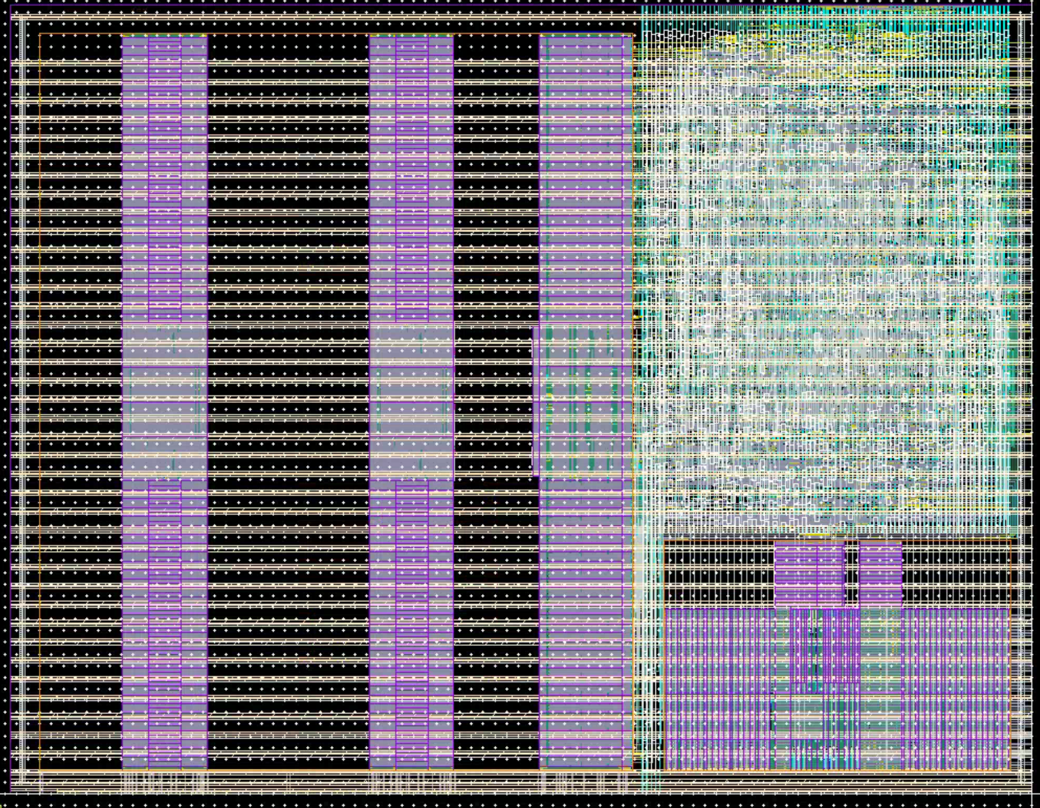
Physical Implementation
Full RTL-to-GDSII layout flow via Synopsys Design Compiler, QuestaSim, Innovus, and Virtuoso
- Clock frequency: 400 MHz (limited by ROM). Underlying logic capable for 500 MHz
- Throughput: 39.8 MS/s
- Area: 0.148 mm², mostly data SRAM
- Precision: 60 dB SQNR, 0.0067% NRMSE
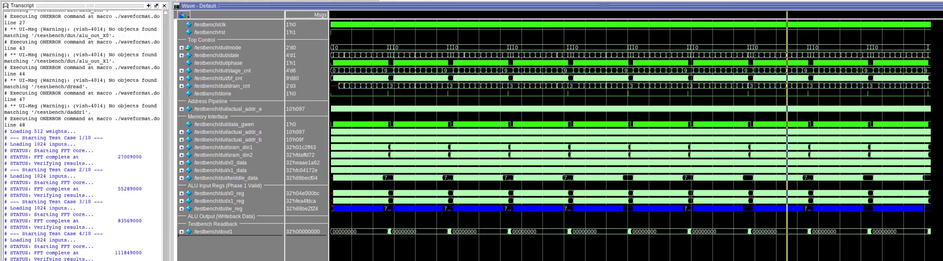
Simulation
- Post-APR Qsim on Python FP golden model and bit-accurate C Int16 model
- Gate-level simulation and power analysis on a subset of inputs